If you need assistance, please send an email to forum at 4hv dot org. To ensure your email is not marked as spam, please include the phrase "4hv help" in the subject line. You can also find assistance via IRC, at irc.shadowworld.net, room #hvcomm.
Support 4hv.org!
Donate:
4hv.org is hosted on a dedicated server. Unfortunately, this server costs and we rely on the help of site members to keep 4hv.org running. Please consider donating. We will place your name on the thanks list and you'll be helping to keep 4hv.org alive and free for everyone. Members whose names appear in red bold have donated recently. Green bold denotes those who have recently donated to keep the server carbon neutral.
Special Thanks To:
Aaron Holmes
Aaron Wheeler
Adam Horden
Alan Scrimgeour
Andre
Andrew Haynes
Anonymous000
asabase
Austin Weil
barney
Barry
Bert Hickman
Bill Kukowski
Blitzorn
Brandon Paradelas
Bruce Bowling
BubeeMike
Byong Park
Cesiumsponge
Chris F.
Chris Hooper
Corey Worthington
Derek Woodroffe
Dalus
Dan Strother
Daniel Davis
Daniel Uhrenholt
datasheetarchive
Dave Billington
Dave Marshall
David F.
Dennis Rogers
drelectrix
Dr. John Gudenas
Dr. Spark
E.TexasTesla
eastvoltresearch
Eirik Taylor
Erik Dyakov
Erlend^SE
Finn Hammer
Firebug24k
GalliumMan
Gary Peterson
George Slade
GhostNull
Gordon Mcknight
Graham Armitage
Grant
GreySoul
Henry H
IamSmooth
In memory of Leo Powning
Jacob Cash
James Howells
James Pawson
Jeff Greenfield
Jeff Thomas
Jesse Frost
Jim Mitchell
jlr134
Joe Mastroianni
John Forcina
John Oberg
John Willcutt
Jon Newcomb
klugesmith
Leslie Wright
Lutz Hoffman
Mads Barnkob
Martin King
Mats Karlsson
Matt Gibson
Matthew Guidry
mbd
Michael D'Angelo
Mikkel
mileswaldron
mister_rf
Neil Foster
Nick de Smith
Nick Soroka
nicklenorp
Nik
Norman Stanley
Patrick Coleman
Paul Brodie
Paul Jordan
Paul Montgomery
Ped
Peter Krogen
Peter Terren
PhilGood
Richard Feldman
Robert Bush
Royce Bailey
Scott Fusare
Scott Newman
smiffy
Stella
Steven Busic
Steve Conner
Steve Jones
Steve Ward
Sulaiman
Thomas Coyle
Thomas A. Wallace
Thomas W
Timo
Torch
Ulf Jonsson
vasil
Vaxian
vladi mazzilli
wastehl
Weston
William Kim
William N.
William Stehl
Wesley Venis
The aforementioned have contributed financially to the continuing triumph of 4hv.org. They are deserving of my most heartfelt thanks.
Registered Member #3414
Joined: Sun Nov 14 2010, 05:05PM
Location: UK
Posts: 4245
OK, so take silicon, for example, it has two electrons in shell 1, 8 in shell 2, and 4 in shell 3. 14 altogether, which maintains an overall neutral charge on the atom, along with the 14 protons. The third shell has space for 18 electrons, but only four spaces are filled. It has four 'valence' electrons, which, in a crystal lattice, it shares with four other silicon atoms, to form basic units of five atoms. There appears to be some confusion on the 'net as to what the lattice structure is. One source describes it as "two interpenetrating face-centered cubic" primitive lattices. Germanium and diamond share the same structure.
In metals, the valence electrons are free to move. If a charge is applied, the electrons move to distribute the charge evenly over the metal, ie electrons will 'flow' along a wire which is connected to a 'source' and a 'drain'.
What happens in silicon (or germanium, for that matter), when a charge is applied?.....This is the bit I don't understand.
(EDIT: It would appear that the electrons in a diode require an energy level of at least ~0.8eV before they will move, but then, only in one direction)
(EDIT: If you squeeze a sponge into the bottle, then fill the bottle to the same level with water, there are some 'holes' in the sponge at the top that are empty. If you then invert the bottle, the holes that were empty fill up, and the holes at the base of the bottle that were full become empty.
In a metal, these 'holes' would be spread evenly throughout the metal, if the metal has an overall positive charge, unless the metal was subjected to a 'large' electric field, when they would be displaced toward one end. (think of a capacitor).
Why, and how, do semi-conductors behave differently?)
Registered Member #1792
Joined: Fri Oct 31 2008, 08:12PM
Location: University of California
Posts: 527
(Now veering pretty far off topic, apologies to thread-starter kimboba, maybe this should be split into a new thread?)
Silicon crystal forms diamond lattice, which happens to also be "two interpenetrating face-centered cubic lattices", and it's called zincblende when the two sub-lattices have different atoms (e.g. Ga and As for GaAs).
The valence shell of Si holds 8 atoms (in hybridized orbitals). Each of the 4 valence electrons enters a bond with another electron from another Si atom so each atom ends up with 8 electrons in its valence shell. Now electrons can only exist in certain specifically allowed energy states, and all of the valence states are filled. If an electric field is applied the electrons and nuclei will feel a force, and they will bend slightly forming a dipole moment (same as any material with a relative dielectric constant > 1) but the electrons won't flow because there is no empty state for them to jump to. It's like LA freeway rush hour.
A small current will actually flow at room temperature because some electrons are excited into the next band of energy states (the conduction band) where most states are empty and so the electrons flow freely, and the holes left behind can also move in an electric field. But there aren't many of these valence band electrons and conduction band holes so the current is relatively small. The populations of these current carriers can be changed dramatically by doping with impurities, among other methods.
Metals are different because their valence bands are not filled, and so when an electric field is applied there are plenty of empty states for electrons to jump to so current easily flows. There are a lot of these electrons so current is large. It's like a freeway that has plenty of space.
wrote ... (EDIT: It would appear that the electrons in a diode require an energy level of at least ~0.8eV before they will move, but then, only in one direction)
Diodes are a different matter because the current is controlled by a potential barrier which is formed as a result of doping the semiconductor into P and N regions. Each P and N region is by itself relatively well conducting because P doping introduces extra valence band holes and N doping introduces extra conduction band electrons. But when you put the two together a potential barrier is formed which is lowered under forward bias and raised under reverse bias. The potential barrier is some fraction of the bandgap which for Si is 1.1eV so when the forward voltage is at the bandgap there should be no barrier to current.
Not following the sponge analogy unforunately.
wrote ... The only difference is that, with the electron, you have a delusion that you understand it. With a hole, you are delusion free. Sounds like +1 for the hole!
Nice way of thinking about it Slack! All of these particle analogies are not how the physicists and material scientists derive the properties of semiconductors, but they are nice enough to come up with effective masses so that the rest of us can pretend =)
Registered Member #3414
Joined: Sun Nov 14 2010, 05:05PM
Location: UK
Posts: 4245
Mattski wrote ...
(Now veering pretty far off topic, apologies to thread-starter kimboba, maybe this should be split into a new thread?)
Although, if you are driving an LED, it's useful to know exactly how it works, but I agree it's not essential to know this in order to drive one.
Mattski wrote ...
Silicon crystal forms diamond lattice, which happens to also be "two interpenetrating face-centered cubic lattices", and it's called zincblende when the two sub-lattices have different atoms (e.g. Ga and As for GaAs).
The valence shell of Si holds 8 atoms (in hybridized orbitals). Each of the 4 valence electrons enters a bond with another electron from another Si atom so each atom ends up with 8 electrons in its valence shell. Now electrons can only exist in certain specifically allowed energy states, and all of the valence states are filled. If an electric field is applied the electrons and nuclei will feel a force, and they will bend slightly forming a dipole moment (same as any material with a relative dielectric constant > 1) but the electrons won't flow because there is no empty state for them to jump to. It's like LA freeway rush hour.
A small current will actually flow at room temperature because some electrons are excited into the next band of energy states (the conduction band) where most states are empty and so the electrons flow freely, and the holes left behind can also move in an electric field. But there aren't many of these valence band electrons and conduction band holes so the current is relatively small. The populations of these current carriers can be changed dramatically by doping with impurities, among other methods.
Metals are different because their valence bands are not filled, and so when an electric field is applied there are plenty of empty states for electrons to jump to so current easily flows. There are a lot of these electrons so current is large. It's like a freeway that has plenty of space.
wrote ... (EDIT: It would appear that the electrons in a diode require an energy level of at least ~0.8eV before they will move, but then, only in one direction)
Diodes are a different matter because the current is controlled by a potential barrier which is formed as a result of doping the semiconductor into P and N regions. Each P and N region is by itself relatively well conducting because P doping introduces extra valence band holes and N doping introduces extra conduction band electrons. But when you put the two together a potential barrier is formed which is lowered under forward bias and raised under reverse bias. The potential barrier is some fraction of the bandgap which for Si is 1.1eV so when the forward voltage is at the bandgap there should be no barrier to current.
Thanks for that description, Mattski. I thought the third shell was 8, and the fourth 10, but a couple of sources said the third was 18, so I thought maybe things had changed since I was at school. Thanks for clearing that up.
I think I can also see how the doping works. Adding impurities will 'mess up' the balance of 8 valence electrons in the third shell, some impurities will result in there not being enough electrons to fill the third shell, etc. It's now all beginning to make sense.
Mattski wrote ...
Not following the sponge analogy unforunately.
wrote ... The only difference is that, with the electron, you have a delusion that you understand it. With a hole, you are delusion free. Sounds like +1 for the hole!
Nice way of thinking about it Slack! All of these particle analogies are not how the physicists and material scientists derive the properties of semiconductors, but they are nice enough to come up with effective masses so that the rest of us can pretend =)
However you look at the analogies, they don't explain 'how' doping 'creates' the extra holes, and I still argue that the holes don't 'move', they are part of the eight valence 'sites' associated with the third shell of each silicon nuclei.
Personally, I see electrons as being a quantum unit, resembling a field with a centre of mass and a centre of charge. Some texts suggest that each electron (and proton, etc) actually extend to fill the universe, however, they each have their own centre of mass and centre of charge (Pauli exclusion principle). (The 'official' size of a proton, for example, is the size which contains a certain percentage of the mass, I forget the exact figures)
Registered Member #2529
Joined: Thu Dec 10 2009, 02:43AM
Location:
Posts: 600
Personally I think there's only one electron, and it fills the universe with a quantum mechanical wave. It's everywhere, but in different amounts. That's why you can't have two electrons in the same place; it's the same electron! But you can have two of the same electron in different places- thanks quantum mechanics!
IRC the doping nicks electrons from the substrate and this creates a hole- the total bulk material is still neutrally charged, but the dope is holding the charge near it, away from the substrate, leaving a hole there (or somewhere nearby). Electrons can fall into the hole, and be pushed out again by other electrons permitting flow.
Registered Member #1792
Joined: Fri Oct 31 2008, 08:12PM
Location: University of California
Posts: 527
wrote ... Thanks for that description, Mattski. I thought the third shell was 8, and the fourth 10, but a couple of sources said the third was 18, so I thought maybe things had changed since I was at school. Thanks for clearing that up.
It's actually somewhat complicated, a free silicon atom has two electrons each in s and p orbitals but when bonded the two types of orbitals combine into sp3 hybridized orbitals... but anyway you end up with several elements or alloys which are semiconducting when the number of valence electrons add up to 8: group IV elements including Germanium, Si, and C, III-V alloys including GaAs, InP, and GaN, II-VI alloys including HgCdTe, and many more besides these.
wrote ... However you look at the analogies, they don't explain 'how' doping 'creates' the extra holes, and I still argue that the holes don't 'move', they are part of the eight valence 'sites' associated with the third shell of each silicon nuclei.
In group IV semiconductors group III like Boron atoms are P-type dopants. One of the 4 boron-silicon bonds only has one electron in it and it can fit another one. Charge is balanced so when the mobile positive hole is formed by an electron jumping onto that bond site there is a fixed negative charge provided by the electron. The electron may leave the boron-silicon bond and go somewhere else but it would be quickly replaced because there's so many electrons in the valence band, and very few holes, so you can basically assume that there will always be an electron there and so you can treat it as a fixed negative charge.
Holes are a theoretical construct (just like electrons as Slack pointed out ;) ) but the essence of a hole which is an empty state in the valence band does indeed move around, so it may start at a p-type dopant site but it will not stay there long and it will move randomly all over the crystal to different atomic sites due to thermal energy.
wrote ... Some texts suggest that each electron (and proton, etc) actually extend to fill the universe, however, they each have their own centre of mass and centre of charge (Pauli exclusion principle). (The 'official' size of a proton, for example, is the size which contains a certain percentage of the mass, I forget the exact figures)
In quantum everything has a wave function which describes the probability that it exists in a certain volume. The wave function only asymptotically approaches 0 as distances go to infinity, but the probability is ludicrously small as you get further and further away from the center of the wavefunction.
However you look at the analogies, they don't explain 'how' doping 'creates' the extra holes, and I still argue that the holes don't 'move', they are part of the eight valence 'sites' associated with the third shell of each silicon nuclei.
Literally you're right, the holes don't move, it just appears that way. If an electron moves to a hole, it fills it and leaves a vacant space where it came from, so the hole is now somewhere else.
In quantum mechanics a many particle state missing an occupant has a lot of similarity to a single particle state. Single particle states are vastly simpler than multi-electron states, so it is a matter of conveniency to talk about holes as 'particles'
Registered Member #72
Joined: Thu Feb 09 2006, 08:29AM
Location: UK St. Albans
Posts: 1659
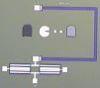
So holes don't move? Take a look at this macroscopic hole below. You can see how it acquires momentum. In order to move the hole, the tiles must move. It is their d(energy)/d(speed) that we see as belonging to the hole. If a tray with 16 tiles is neutral, then the tray itself must have a total charge of -16 tiles. The hole you can see therefore 'uncovers' a charge of -1 tile.
And holes aren't real QM particles? They are every bit as 'real' as QM 'electrons' in a conductor or semi-conductor. Conductivity electrons, if you design experiments to look at their particle behaviour, have a different mass to free electrons, you can think of it as due to their interaction with the lattice. Other 'real' QM particles include phonons (quantised lattice vibrations), and the really improbable and screwy photon.
So holes don't move? Take a look at this macroscopic hole below. You can see how it acquires momentum. In order to move the hole, the tiles must move. It is their d(energy)/d(speed) that we see as belonging to the hole.
That is just the point I was trying to make. The hole mass is derived from the movement of electrons. Electrons must be moved in order for holes to move.
Conductivity electrons, if you design experiments to look at their particle behaviour, have a different mass to free electrons, you can think of it as due to their interaction with the lattice.
I agree with this. Giving electrons in a lattice a different mass than that of free electrons takes into account their lattice interaction. In this way you can more easily describe their behaviour and don't have to account for their interaction explicitly. In a full calculation, which includes lattice interactions, you would need to use the free electron mass.
Registered Member #30
Joined: Fri Feb 03 2006, 10:52AM
Location: Glasgow, Scotland
Posts: 6706
Can anyone explain along these lines why the mobility of holes is different to the mobility of electrons? Surely if a hole is just an "absence of electron", then moving one hole is the same as moving one electron, so it ought to have the same mobility.
But in practice the mobility of holes is less, and P-channel MOSFETs, where the current is carried by holes, never perform quite as well as their N-channel counterparts.
Registered Member #2529
Joined: Thu Dec 10 2009, 02:43AM
Location:
Posts: 600
When the bands are nearly full, hole conduction dominates, the holes are found in higher bands, which have a different structure, lower mobility. When they're emptier, lower energy, higher mobility bands are available and then electrons flow more easily.
This site is powered by e107, which is released under the GNU GPL License. All work on this site, except where otherwise noted, is licensed under a Creative Commons Attribution-ShareAlike 2.5 License. By submitting any information to this site, you agree that anything submitted will be so licensed. Please read our Disclaimer and Policies page for information on your rights and responsibilities regarding this site.


 Driving a led with mains.