
"Flyback" Mode Flyback Driver Design
Mr.Warwickshire, Thu Jul 06 2017, 10:25PMHello everyone! This is my first post on the forum here. Anyways, after researching the archives on this forum and other websites I believe I have designed the most stable 555 "flyback" mode driver. Here's a picture of my block diagram hybrid schematic. Any issues with it?
Picture:

Re: "Flyback" Mode Flyback Driver Design
Hazmatt_(The Underdog), Fri Jul 07 2017, 04:22AM
Your flyback will work better in the 10-20% duty cycle range. You're assuming flybacks work well with 50% duty and that just causes a lot of heat buildup in the switches (Mosfets).
You really don't need 2 mosfets either, one is ample, but it's really up to you how hard you want to push the flyback.
I would also get rid of the capacitor across the flyback winding, it will probably smoke or arc over during tuning.
Re: "Flyback" Mode Flyback Driver Design
Mr.Warwickshire, Fri Jul 07 2017, 05:59AM
I should be able to run the circuit at 10 to 20 percent duty cycle with a 555. Doesn't the capacity across the primary increase efficiency? I thought that's what made it quasi resonant.
Mr.Warwickshire, Fri Jul 07 2017, 05:59AM
I should be able to run the circuit at 10 to 20 percent duty cycle with a 555. Doesn't the capacity across the primary increase efficiency? I thought that's what made it quasi resonant.
Re: "Flyback" Mode Flyback Driver Design
Sulaiman, Fri Jul 07 2017, 06:53AM
What will be the main use of the circuit ?
1 constant voltage and current/power
2 capacitor charging
3 arcs
Each has different requirements of the flyback inverter.
In my opinion, a capacitor across the primary with the frequency chosen for resonance is only useful for #3
Regarding frequency, duty eyc.
. ON time determines peak current in the primary (Ip = Vdc x Ton/Lpri)
hence the energy available for each cycle (0.5 x Lp x Ip x Ip)
and (output power) = (energy per cycle) x (cycles per second)
.OFF time is required to allow the energy stored in the flyback magnetic field to discharge into the load via the secondary winding,
one way to determine the minimum time required is Toff >= Ton x (dc supply voltage) / (primary flyback voltage)
and (primary flyback voltage) = (secondary output voltage) / (flyback transformer sec : pri turns ratio)
The off time can be increased above this minimum to reduce output power and frequency,
So it is common to have a short ON time and long OFF time for low power
and a long ON time with short OFF time for high power
If the ON time is too long then something will die due to over-current
If the OFF time is too short then something will die due to over-current
If you use a resonant capacitor on the primary then the frequency should be fixed at the resonant frequency and the duty cycle adjusted for power control.
(use pin3 instead of pin7 to drive the timing section, e.g.
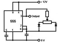
(copied from the above link without permission)
When a flyback is used to charge a high voltage capacitor starting from near zero voltage across the capacitor
the capacitor will typically charge over many 10's of flyback cycles
so during each cycle of charging and discharging the high voltage capacitor
the OFF time should be long at the beginning of the charging cycle and short at the end.
This is the main weakness of a 555 based flyback inverter
great for fixed voltage and current output, not so good for capacitor charging.
I do not like to see all three terminals of transistors paralleled as it OFTEN causes r.f. oscillations that heat up the transistors
the frequency of oscillation is often above the capabilities of my 20 MHz 'scope !
So even if only switching at low frequencies, use separate gate/base drive resistors/networks as a habit.
One big problem with 555-flyback inverters is
what happens when energy is pumped into the primary every cycle but there is no load on the eht output ?
(this is important to understand and design for, in my opinion)
Also, notice that for a given Ton and Toff, the POWER is fixed
output power is volts x amps
so if either is changed, the other will change to maintain constant POWER.
Despite all of these considerations, I still like the 555 flyback for its simplicity
and because unlike most smps ICs it will be available in dil packages for a long time
and a 0.1" pitch dil IC is a lot easier to play with than a micro.mini.nano-scopic smd IC
P.S. I always try to have the lowest operating frequency of the inverter well above the highest frequency that I can hear.
(hence I rarely use automotive ignition coils even though I like their ruggedness)
Your crt flyback transformer secondary will have an intrinsic self-resonant frequency well above audio,
a large resonance capacitor could easily reduce the resonant frequency into the audio range,
which is cool for a while - then it becomes VERY irritating.
P.P.S. For most mosfet or igbt transistors a separate gate drive circuit is unneccessary as the gate loading is mainly capacitive which is no problem for the 555.
If available, use one suitable transistor rather than two 1/2 -suitable ones in parallel.
For the snubber I prefer the DCR type, have a look at Figure 2 here
as an added bonus, if the capacitor has sufficient capacitance you get a (very dangerous and/or painful) high voltage supply
with voltage of Vdc + (primary flyback voltage)
Sulaiman, Fri Jul 07 2017, 06:53AM
What will be the main use of the circuit ?
1 constant voltage and current/power
2 capacitor charging
3 arcs
Each has different requirements of the flyback inverter.
In my opinion, a capacitor across the primary with the frequency chosen for resonance is only useful for #3
Regarding frequency, duty eyc.
. ON time determines peak current in the primary (Ip = Vdc x Ton/Lpri)
hence the energy available for each cycle (0.5 x Lp x Ip x Ip)
and (output power) = (energy per cycle) x (cycles per second)
.OFF time is required to allow the energy stored in the flyback magnetic field to discharge into the load via the secondary winding,
one way to determine the minimum time required is Toff >= Ton x (dc supply voltage) / (primary flyback voltage)
and (primary flyback voltage) = (secondary output voltage) / (flyback transformer sec : pri turns ratio)
The off time can be increased above this minimum to reduce output power and frequency,
So it is common to have a short ON time and long OFF time for low power
and a long ON time with short OFF time for high power
If the ON time is too long then something will die due to over-current
If the OFF time is too short then something will die due to over-current
If you use a resonant capacitor on the primary then the frequency should be fixed at the resonant frequency and the duty cycle adjusted for power control.
(use pin3 instead of pin7 to drive the timing section, e.g.


(copied from the above link without permission)
When a flyback is used to charge a high voltage capacitor starting from near zero voltage across the capacitor
the capacitor will typically charge over many 10's of flyback cycles
so during each cycle of charging and discharging the high voltage capacitor
the OFF time should be long at the beginning of the charging cycle and short at the end.
This is the main weakness of a 555 based flyback inverter
great for fixed voltage and current output, not so good for capacitor charging.
I do not like to see all three terminals of transistors paralleled as it OFTEN causes r.f. oscillations that heat up the transistors
the frequency of oscillation is often above the capabilities of my 20 MHz 'scope !
So even if only switching at low frequencies, use separate gate/base drive resistors/networks as a habit.
One big problem with 555-flyback inverters is
what happens when energy is pumped into the primary every cycle but there is no load on the eht output ?
(this is important to understand and design for, in my opinion)
Also, notice that for a given Ton and Toff, the POWER is fixed
output power is volts x amps
so if either is changed, the other will change to maintain constant POWER.
Despite all of these considerations, I still like the 555 flyback for its simplicity
and because unlike most smps ICs it will be available in dil packages for a long time
and a 0.1" pitch dil IC is a lot easier to play with than a micro.mini.nano-scopic smd IC
P.S. I always try to have the lowest operating frequency of the inverter well above the highest frequency that I can hear.
(hence I rarely use automotive ignition coils even though I like their ruggedness)
Your crt flyback transformer secondary will have an intrinsic self-resonant frequency well above audio,
a large resonance capacitor could easily reduce the resonant frequency into the audio range,
which is cool for a while - then it becomes VERY irritating.
P.P.S. For most mosfet or igbt transistors a separate gate drive circuit is unneccessary as the gate loading is mainly capacitive which is no problem for the 555.
If available, use one suitable transistor rather than two 1/2 -suitable ones in parallel.
For the snubber I prefer the DCR type, have a look at Figure 2 here

as an added bonus, if the capacitor has sufficient capacitance you get a (very dangerous and/or painful) high voltage supply
with voltage of Vdc + (primary flyback voltage)
Re: "Flyback" Mode Flyback Driver Design
Mr.Warwickshire, Fri Jul 07 2017, 03:49PM
The main purpose of this driver is to achieve the highest voltage possible.current can come second. I have a very nice half bridge driver but I get all current with decent voltages. Oh and I plan on using this to drive both ac and DC flyback.
EDIT: My 555 circuit has both variable frequency and duty cycle. So I don't think I need to use that other method although it seems a little more stable/professional.
Re: "Flyback" Mode Flyback Driver Design
Sulaiman, Fri Jul 07 2017, 04:04PM
For the highest seondary voltage possible, you will be limited by one of these constraints;
. insulation of the flyback transformer secondary
. load on secondary
. voltage rating of flyback transistor must be more than (dc supply voltage) + (peak output voltage / transformer turns ratio)
Re: "Flyback" Mode Flyback Driver Design
Mr.Warwickshire, Fri Jul 07 2017, 04:14PM
I have purchased both 600v misfits and igbts along with 200v ones. So I should be fine. And shouldn't the TVS's in my design protect the transistors. I bought some that breakdown at 170 volts. As for the flyback insulation, I have 3d printed bobbins for ac flyback which look like your typical inverter stype XRT. They will be immersed in oil.
Re: "Flyback" Mode Flyback Driver Design
Mr.Warwickshire, Fri Jul 07 2017, 04:31PM
Here it the new schematic.

Mr.Warwickshire, Fri Jul 07 2017, 04:31PM
Here it the new schematic.

Re: "Flyback" Mode Flyback Driver Design
Sulaiman, Fri Jul 07 2017, 04:55PM
looks like a plan ... good luck and have fun.
Before testing the whole circuit, replace the flyback transformer primary with a suitable filament lamp,
you will be able to see the effect of duty cycle by lamp brightness if all is well.
P.S. probably not useful but this arrangement needs only three wires to the transformer for easier insulation / mounting
Re: "Flyback" Mode Flyback Driver Design
Mr.Warwickshire, Fri Jul 07 2017, 05:01PM
Alright, thanks for the help. I will post pictures if working.
Mr.Warwickshire, Fri Jul 07 2017, 05:01PM
Alright, thanks for the help. I will post pictures if working.
Re: "Flyback" Mode Flyback Driver Design
Sulaiman, Fri Jul 07 2017, 05:25PM
it would be more fun to watch a video of the first time that you test it ;)
videography example
Sulaiman, Fri Jul 07 2017, 05:25PM
it would be more fun to watch a video of the first time that you test it ;)
videography example

Re: "Flyback" Mode Flyback Driver Design
Mr.Warwickshire, Fri Jul 07 2017, 10:42PM
It ran okay first try with an IRFP260N. Only problem was that the TVS diode across the mosfet was getting HOT.
Mr.Warwickshire, Fri Jul 07 2017, 10:42PM
It ran okay first try with an IRFP260N. Only problem was that the TVS diode across the mosfet was getting HOT.
Re: "Flyback" Mode Flyback Driver Design
Sulaiman, Sat Jul 08 2017, 08:47AM
There are two likely causes for the TVS heating;
1) each cycle the capacitance of the TVS is charged and discharged, the resultant charging and discharging currents heat up any resistive/lossy parts of the circuit
- the TVS and the transistor.
This loss/heating can be eliminated by putting a suitable diode in series with the TVS.
2) A more significant source of your TVS heating is probably
Sulaiman wrote ...
One big problem with 555-flyback inverters is
what happens when energy is pumped into the primary every cycle but there is no load on the eht output ?
(this is important to understand and design for, in my opinion)
One big problem with 555-flyback inverters is
what happens when energy is pumped into the primary every cycle but there is no load on the eht output ?
(this is important to understand and design for, in my opinion)
Re: "Flyback" Mode Flyback Driver Design
Hazmatt_(The Underdog), Sat Jul 08 2017, 05:06PM
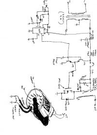
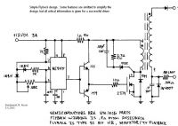
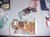
here's my design I did in 2005 for design comparison if you want.
This was designed for lower power to drive a Crooke's tube without generating too much X-ray for the kids science center. We had a hard time keeping
the tube ignited because it was over 80 years old.
If you want lots of power, you need to design for a push-pull, half bridge, or full bridge and use something like the SG3525 or TL494.
Anyway, hope this helps.


Re: "Flyback" Mode Flyback Driver Design
Mr.Warwickshire, Sun Jul 09 2017, 02:17AM
Okay thanks for the schematics. I have replaced the IRFP260 with a 600v 50amp mosfet. I tested it and it works great with nearly zero heating of the transistor. I don't need the TVS either (atleast not until 50+ volt input) so I don't have to worry about it melting. BUT when I do run it above 50v I will try putting the diode in series with the TVS to see if that helps. I have yet to try it on a dc flyback. Just my hand wound AC ones. My DIY high frequency XRT works amazing on this driver. There is about 3-4cm of corona coming off the output wire when I run it at 25ish volts. I'll see if I can get a picture of it and post it on the projects section. Thanks for the help!
Print this page