SSTC Halfbridge PCB Design
Phil33ts, Sun Apr 03 2016, 11:12AMHello all.
I have already made one SSTC and it worked with 230V but the design was not perfect.
I'd like to make a new SSTC, using IGBT, and design my own PCB layout for that.
I am using Eagle and I've already made and etched several PCBs
I am using single-sided PCB and this topic is only about them.
I know that PCB layout is important and must be designed carefully. But I don't know what exacly matters and how to place components correctly. And here is the beginning of my trouble:
1. How should be the SSTC PCB designed? What are the design rules of high frequence PCB? Can anyone give me some hints or show me some online courses, e-books, pdfs or youtube videos that are revelant to this topic?
2. Is there any "professional" or at least "well made" SSTC PCB layout available that I can learn from? Can any of you guys publish your own layouts?
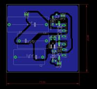
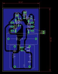
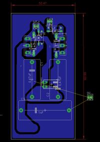
3. Please take a look here, those are my ideas for IGBT halfbridge PCB:
Schematic:

Layout A:

Layout B:

Layout C:

Which of the layouts is the best and how can I improve it more?
4. Regarding this IGBT halfbridge, what should be closer to IGBT pins? Snubber capacitor (single, big one) or those two caps?
5. When I make a GDT driver, what should be placed next to TC44** (MOSFET driver) pins - tantalum capacitor 47uF or 100nF ceramic one?
Thanks in advance. I will publish my Eagle project files when I finish this SSTC project.
Re: SSTC Halfbridge PCB Design
Erlend^SE, Sun Apr 03 2016, 12:37PM
I would generally suggest doing all the power connections with the polygon function, trying to cover as much area as possible.
I would suggest doing a single heatsink, gdt on one side, and power routing on the other side of the heatsink. Mixing them give a chance of induction to gate that is undesired.
If you can, do 2-sided so you can use more of the area for power.
Re: SSTC Halfbridge PCB Design
loneoceans, Sun Apr 03 2016, 06:00PM
Check out my half bridge and full bridge SSTCs designed for a single PCB. :) See my layouts here:
SSTC 4:
SSTC 3:
With a PCB you essentially gain the benefit of easy double sided buses, so the usual practice is to keep the main bus as low inductance as possible by keeping them laminated (top and bottom layer) to the bus caps. Typically that's what I do, with the outputs breaking out at the sides. Likewise with the gate drive, always good to keep the loop inductance as low as possible of the gate drive traces to the GDT - using SMD components helps as well.
loneoceans, Sun Apr 03 2016, 06:00PM
Check out my half bridge and full bridge SSTCs designed for a single PCB. :) See my layouts here:
SSTC 4:

SSTC 3:

With a PCB you essentially gain the benefit of easy double sided buses, so the usual practice is to keep the main bus as low inductance as possible by keeping them laminated (top and bottom layer) to the bus caps. Typically that's what I do, with the outputs breaking out at the sides. Likewise with the gate drive, always good to keep the loop inductance as low as possible of the gate drive traces to the GDT - using SMD components helps as well.
Re: SSTC Halfbridge PCB Design
Phil33ts, Fri Apr 08 2016, 08:48AM
I already know your site and I think that your PCBs are good but I'd like to see more examples.
The idea of fitting everything into ATX case is very nice but I don't know if I can achieve it with single-sided board. Anyway, loneoceans, speaking of your SSTCs, how did you choose the 230->12V transformer? I mean, how do I know how much power is required for logic circuit to drive?
You have used VPP12-400 transformer for both SSTCs and it had enough power?
Print this page