
Need help about Richie burnnet schematic on sstc
rajheman, Tue Jul 07 2015, 05:30PMHello friends myself raj from India ..basically I deal with chemistry. Myself also interested in electronics .but I have little knowledge about electronics. I have attracted a lot to sstc . so thats why I followed the Richie burnnet schematic to make sstc .
sstc01.gif

sstc02.gif

I made the circuit as it is. As mentioned by Richie burnnet. Please see the pictures. But it didn't work .please suggest me to make a working sstc. I heard that oscilloscope is important to check the circuit. Can plz help to where and how to check the circuit with oscilloscope.
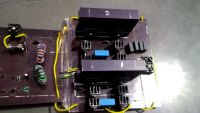
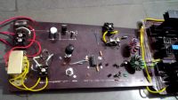
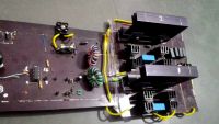
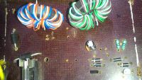
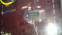
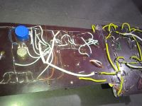
Re: Need help about Richie burnnet schematic on sstc
zzz_julian_zzz, Wed Jul 08 2015, 03:23AM
Remove first the POWER STAGE supply (i.e. disconnect it from AC mains), make sure that you are using isolation type transformer in supplying your CONTROL STAGE like in the schematics (otherwise your oscilloscope might get damaged)
1. check first if there is power going to your IC (TL494).
I presume that you followed everything in the schematic, so you can connect the Positive probe of Volt meter to PIN 12,11 OR 8 and connect the Negative probe to PIN 1,7, OR 16. See if there is 12vdc coming to these pins.
2. Use oscilloscope to check the Oscillating output. Connect Lead Probe of the oscilloscope to PIN 9 OR 10, and connect the Ground Probe to Pin 1,7 or 16. Make sure that the oscillating Frequency is being/can be read by the time division setting of your oscilloscope (for 350 kHz, you can use 0.1us/div) You should see square waves coming from this pins.
3. Check Gate Drive Output, from Richie's schematic, Disconnect first the Gate Drive Transformer. Connect the Oscilloscope Lead Probe to (before 10uf capacitor going to) POINT A, and the Ground Probe to ground or PIN 1, or PIN 7. Do this also to POINT B (after the resistor). You should see identical square waves from instruction number 2.
4. If above procedures are Okay, check gate waveform:
using only 1 channel of the oscilloscope, connect lead probe to gate pin and ground probe to source pin of the MOSFET lower left side first (from your schematic) and then DO THIS TO ALL MOSFET 1 BY 1.
5. check the phasing (LEFT LEG OF AC):
this is to ensure that the POWER STAGE is indeed creating a square wave across the load (primary coil/resonator).
to do this, AGAIN W/O connecting to AC mains, using 2 channels of the oscilloscope,
a. channel 1: check the GATE wave form of TOP LEFT MOSFET by connecting the lead probe to the gate pin and connecting the ground probe to its source pin
b. channel 2: check the GATE wave form of LOWER LEFT MOSFET by connecting the lead probe to the gate pin and connecting the ground probe to its source pin
you should see on the oscilloscope channels those semi square wave that is OUT-OF-PHASE in oscillation. means, above MOSFET is on, lower MOSFET is off, and vice versa.
6. check the phasing (RIGHT LEG OF AC):
this is to ensure that the POWER STAGE is indeed creating a square wave across the load (primary coil/resonator).
to do this, AGAIN W/O connecting to AC mains, using 2 channels of the oscilloscope,
a. channel 1: check the GATE wave form of TOP RIGHT MOSFET by connecting the lead probe to the gate pin and connecting the ground probe to its source pin
b. channel 2: check the GATE wave form of the LOWER RIGHT MOSFET by connecting the lead probe to the gate pin and connecting the ground probe to its source pin
you should see on the Channels simultaneously those semi square wave that is OUT-OF-PHASE in oscillation. means, above MOSFET is on, lower MOSFET is off, and vice versa.
7. Phase check for left and right AC leg:
now we know that the left side MOSFETS of the bridge and the right side MOSFETS of your bridge are out-of-phase, you must now check if these legs are OK. meaning, TOP MOSFETs are out-of-phase and LOWER MOSFETs are out-of-phase too:
a. channel 1: check the GATE wave form of TOP RIGHT MOSFET by connecting the lead probe to the gate pin and connecting the ground probe to its source pin
b. channel 2: check the GATE wave form of the TOP LEFT MOSFET by connecting the lead probe to the gate pin and connecting the ground probe to its source pin
you should also see OUT-OF-PHASE oscillation here.
Please do these procedures first. thanks and good luck troubleshooting!
Re: Need help about Richie burnnet schematic on sstc
rajheman, Wed Jul 08 2015, 07:21AM
Thanks a lot for giving your valuable suggestions Mr.Julian . soon I vl follow the process and I vl post here my working sstc :)
rajheman, Wed Jul 08 2015, 07:21AM
Thanks a lot for giving your valuable suggestions Mr.Julian . soon I vl follow the process and I vl post here my working sstc :)
Re: Need help about Richie burnnet schematic on sstc
rajheman, Wed Jul 15 2015, 03:23PM
In Richie burnnet schematic he mentioned
Zxt450 60v,1amp 1wat npn transistor
Ztx550 60v,1amp 1wat PNP transistor
VN10KM 60v 0.31 amp N channel MOSFET
But I used
Ztx651 60v,2amp 1wat npn transistor
Ztx752 60v,2amp 1wat PNP transistor
BSN274 270v 25 amp N channel MOSFET
In my circuit
And also I can't get STW15NB50 MOSFET, so instead of it I used IRFP460
Are this substitutes work ????
Re: Need help about Richie burnnet schematic on sstc
rajheman, Wed Jul 15 2015, 03:28PM
One more information please.
Would it is necessary to keep the primary winding of sstc is in same direction to secondary winding of sstc ???
Is it matters ..I mean does it show any effect on out put of sstc ???
rajheman, Wed Jul 15 2015, 03:28PM
One more information please.
Would it is necessary to keep the primary winding of sstc is in same direction to secondary winding of sstc ???
Is it matters ..I mean does it show any effect on out put of sstc ???
Re: Need help about Richie burnnet schematic on sstc
zzz_julian_zzz, Mon Jul 20 2015, 05:55AM
Hi Rajheman,
I checked the replacement transistor you suggested. And yes, they can all work as expected for their part. Good job on finding those replacements! :)
BTW, BSN274 is 0.25 Amp, not 25 Amp
Be sure to put bypass capacitor across the power supply rails. In here, the 470n / 275 VAC polypropelene capacitors are critical!
You can use higher than these, range from 1uf to 10uf (MYLAR caps are more common - at least 350VDC) and they also work pretty well. They are to protect your IRFP460 from voltage spikes. So the closer the CAPS to the MOSFET, the better. Put DC blocking capacitor as well, those are the 4x220n 275VAC in the diagram (total of 880 nf) note that if you use too high of capacitance 2-5uf will cause higher current in your primary circuit. I think one of the reason is that it is because it has now lower impedance (BIG Capacitance, SMALL L inductance).. BUT,. if you use too small of C, you might make the circuit close to the resonant frequency and eat up higher energy (and damps the energy to the secondary LIKE a DRSSTC, but in your circuit, you are not using an interrupter so the ringing will not be limited until the MOSFET cannot handle the current anymore. It will be very dangerous for your MOSFET if that happens.
I made at least 5 resonators with different winding orientation but never had issues with it. So I guess it's not that critical.
zzz_julian_zzz, Mon Jul 20 2015, 05:55AM
Hi Rajheman,
I checked the replacement transistor you suggested. And yes, they can all work as expected for their part. Good job on finding those replacements! :)
BTW, BSN274 is 0.25 Amp, not 25 Amp
Be sure to put bypass capacitor across the power supply rails. In here,
 the 470n / 275 VAC polypropelene capacitors are critical!
 You can use higher than these, range from 1uf to 10uf (MYLAR caps are more common - at least 350VDC) and they also work pretty well. They are to protect your IRFP460 from voltage spikes. So the closer the CAPS to the MOSFET, the better. Put DC blocking capacitor as well, those are the 4x220n 275VAC in the diagram (total of 880 nf) note that if you use too high of capacitance 2-5uf will cause higher current in your primary circuit. I think one of the reason is that it is because it has now lower impedance (BIG Capacitance, SMALL L inductance).. BUT,. if you use too small of C, you might make the circuit close to the resonant frequency and eat up higher energy (and damps the energy to the secondary LIKE a DRSSTC, but in your circuit, you are not using an interrupter so the ringing will not be limited until the MOSFET cannot handle the current anymore. It will be very dangerous for your MOSFET if that happens.
I made at least 5 resonators with different winding orientation but never had issues with it. So I guess it's not that critical.
Print this page