
An attempt at a QCW DRSSTC design
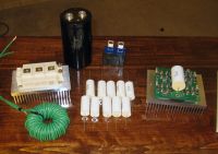
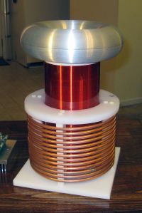
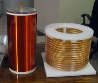
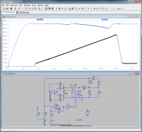
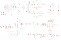
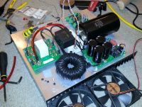
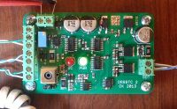
cjk2, Tue Jan 01 2013, 01:15AMI have been wanting to build one of these for a while now. I will be attempting to use the bang-bang control method that everyone else has had success with. Here are some pictures of what I have so far. The schematic is for the buck converter. The secondary geometry is a copy of what Eric Goodchild used as far I could tell.
Re: An attempt at a QCW DRSSTC design
Physics Junkie, Tue Jan 01 2013, 03:42AM
Very nice looking. What are specs on that green cable for the GDT? (i assume its the gdt) Looks pretty heavy duty from the image.
Physics Junkie, Tue Jan 01 2013, 03:42AM
Very nice looking. What are specs on that green cable for the GDT? (i assume its the gdt) Looks pretty heavy duty from the image.
Re: An attempt at a QCW DRSSTC design
cjk2, Tue Jan 01 2013, 05:33AM
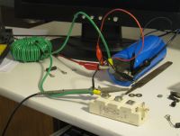
The toroid with the green wire is for the inductor for the buck converter. It is 65 turns of 10 AWG wire on a T300-2D powered iron core. It measures about 95 uH.
Everyone else uses gaped ferrite for this inductor. I was not able to find any cheap and large ferrite cores to wind my inductor on so I went with a toroid. Type 2 material has a low permeability so will not saturate even at a few hundred amps. Because of this the inductor does not require any added air gap.
It is possible that the core will be too lossy but I suspect it may well work. I also considered using an air core but I decided that the leakage would be too high and may cause interference with the control electronics.
Re: An attempt at a QCW DRSSTC design
Goodchild, Tue Jan 01 2013, 05:27PM
All your power electronics and secondary look great, very clean, and well made BTW! Much better than my first QCW setup.
Are you sure it's not going to saturate at a couple hundred amps? Seems a little pie in the sky for a core of that size.
If you haven't already I would do a saturation test on your inductor. Rig up an SCR, large electrolytic , PSU and current shunt. Fill the cap up to say 30 or 50V with the PSU and discharge it into the inductor with the SCR and watch the resulting current waveform through the inductor with the current shunt on a scope.
For ferrite you will see something like this
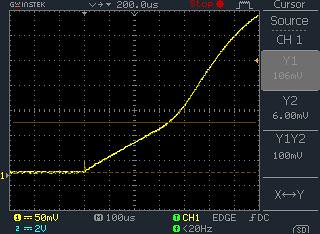
The knee in the current is the saturation point in which the inductance starts to roll off.
For powdered iron the role off will be much slower. But generally after it has rolled off enough to stop properly filtering you will start to see problems. Due to the buck drive frequency mixing with the inverter frequency and causing havoc with your primary feedback.
Just out of curiosity what is the value of your filter cap on your buck and what frequency is it going to run at?
Goodchild, Tue Jan 01 2013, 05:27PM
All your power electronics and secondary look great, very clean, and well made BTW! Much better than my first QCW setup.
Are you sure it's not going to saturate at a couple hundred amps? Seems a little pie in the sky for a core of that size.
If you haven't already I would do a saturation test on your inductor. Rig up an SCR, large electrolytic , PSU and current shunt. Fill the cap up to say 30 or 50V with the PSU and discharge it into the inductor with the SCR and watch the resulting current waveform through the inductor with the current shunt on a scope.
For ferrite you will see something like this

The knee in the current is the saturation point in which the inductance starts to roll off.
For powdered iron the role off will be much slower. But generally after it has rolled off enough to stop properly filtering you will start to see problems. Due to the buck drive frequency mixing with the inverter frequency and causing havoc with your primary feedback.
Just out of curiosity what is the value of your filter cap on your buck and what frequency is it going to run at?
Re: An attempt at a QCW DRSSTC design
Sulaiman, Tue Jan 01 2013, 05:52PM
Don't know if it helps but I calculate 2.55 A in that inductor for 100 gauss = 0.01 T
(2.55A pk @ 500 kHz to 1 MHz, 10Apk @ 50 kHz to 100 kHz etc.)
More likely to melt the insulation than saturate the core I guess.
(from L=N.phi/I, phi = B.Ae, and L=Al.N^2 ... NI = B.Ae/Al)
Re: An attempt at a QCW DRSSTC design
cjk2, Tue Jan 01 2013, 08:16PM
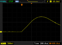
Eric, I did the test you suggested and found no signs of saturation. I only charged my cap to 36V so I was only able to push about 100A through this inductor before the cap was out of energy.
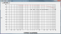
Simulation confirms that it takes a lot of current to saturate this material.
From the slope of the graph (100A in 368 uS) I calculated the inductor has a value of 128 uH. I also measured the inductance by resonating it with a 100 nF cap and found a value of about 95 uH. The simulation seems to suggest I should have about 100 uH at DC. Who knows which number is really right but any of these values would be reasonable.
I used a 0.01 Ohm shunt resistor and a 1X probe so the scope shows 50A per division. I did not have a big SCR so I used half of an IGBT brick to do the switching.
The only concern I have now is excessive loss in the core material.
I plan on using 25 uF of total filter capacitance on the output of the buck converter. This includes the decoupling capacitor across the full bridge. LT spice simulation shows the max operating frequency of the buck converter is about 30 kHz.


Re: An attempt at a QCW DRSSTC design
Goodchild, Thu Jan 03 2013, 07:31AM
Well go figure, that's one heck of a core for it's size! Looks like it started to roll off at around 125A more than plenty for that bridge. I guess all you have to worry about is the looseness, but hey it's hobby grade so long as it's not on fire, exploding, melting, smoking, or glowing it's working (for the most part).
You may also find that you can run faster on that semikron, I found rather low switching losses with CM300 and CM600s in my buck even running close to 60KHz and they are way slower than those semikrons.
Keep us updated I look forward to seeing it run!
Goodchild, Thu Jan 03 2013, 07:31AM
Well go figure, that's one heck of a core for it's size! Looks like it started to roll off at around 125A more than plenty for that bridge. I guess all you have to worry about is the looseness, but hey it's hobby grade so long as it's not on fire, exploding, melting, smoking, or glowing it's working (for the most part).

You may also find that you can run faster on that semikron, I found rather low switching losses with CM300 and CM600s in my buck even running close to 60KHz and they are way slower than those semikrons.
Keep us updated I look forward to seeing it run!
Re: An attempt at a QCW DRSSTC design
cjk2, Mon Jan 07 2013, 06:34PM
Eric, looking at the design of the buck converter you have on your website I see you use a FOD3184 to drive each of the IGBTs. Did you ever find that these overheat? I suspect that each gate of my IGBT brick will be about 15nF. This is a fairly large load to drive at say 50kHz. I would like to be able to run my buck converter continuously and have it put out say 150V and not have the IGBT driver section overheat.
I currently have an IXDI604SIA selected to drive each IGBT gate and two IXDI604SIA's in a full bridge to drive the transformer for my isolated gate supply.
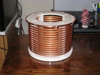
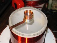
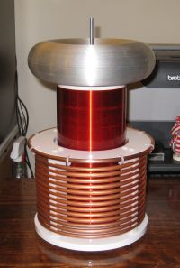
I went ahead and had some of the parts of the primary laser cut out of 1/4" white acrylic.


Re: An attempt at a QCW DRSSTC design
Goodchild, Mon Jan 07 2013, 08:43PM
My gate drivers never overheated, matter in fact they worked rather well all the way up to about 70KHz. I picked those drivers because they had the opto for the high side driver already built in and they are rated to 9A if I remember right. Your bricks are also going to have a much lower gate C than the IGBTs I used in my buck. What I really had trouble with was the the linear V-regs I used to provide the 24V to the gate drive chips. They overheated on occasion and in hindsight it would have been a good idea to go with a custom SMPS to provide the isolated 24V rails.
Re: An attempt at a QCW DRSSTC design
teravolt, Tue Jan 08 2013, 05:02AM
I prefer the IXDD614CI because it is a TO-220 package and can easily be heat sunck. Dip packages can't despite the amount of switching cycles it takes for continuous duty. each time the gate chip is between switch cycle the ic is in a linear state and those dips cant store the heat. I use isolated transformer supplies instead of a buck converter type supply and fiber optics instead of optos. f/o's are a little more expensive than opto's but I feel that it is cleaner. I can run these boards to 500khz, usually the IGBT's can't keep up. if you want a circuit it is easy to make.
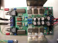
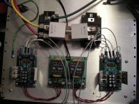
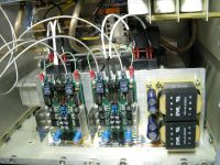


Re: An attempt at a QCW DRSSTC design
cjk2, Sun Feb 10 2013, 05:47AM
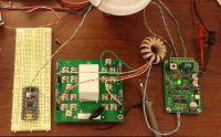
I have done lots more work on this design.
The buck converter works pretty well as far as I have tested it. The board will be redesigned soon as the current one gets warmer than I would like.
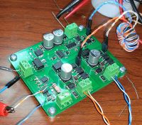
I am having problems with the self resonant full bridge driver. I believe I have shoot through problems. my output stage is a full bridge of two FDD8424 driven by an IXDI604. The circuit looks similar to Steve Ward's UD 2.1 seen here: http://www.stevehv.4hv.org/leadcomp/UD2_1revB/UD2_1revbschem.pdf.
I was running the driver CW from a function generator to test. At 320 Khz, I see a current draw of 70 ma with no load on my GDT. With the gate of one IGBT connected, the current draw goes up to 450 ma. I expect to see about 250 ma in this case so I suspect something is wrong with my output stage.
Any ideas?


Re: An attempt at a QCW DRSSTC design
zzz_julian_zzz, Fri May 17 2013, 03:55AM
Hi Cjk2,
Just wondering on your schematic, you put the positive 5V on the 4th pin of MCP6562 which is based on the datasheet, it is the Negative rail of the this IC. Same with the 8th pin - connected on the ground. ( Which in the DS it is the positive rail).. Isn't its just a misconnection/wrong pin config? thanks.
zzz_julian_zzz, Fri May 17 2013, 03:55AM
cjk2 wrote ...
I have been wanting to build one of these for a while now. I will be attempting to use the bang-bang control method that everyone else has had success with. Here are some pictures of what I have so far. The schematic is for the buck converter. The secondary geometry is a copy of what Eric Goodchild used as far I could tell.


I have been wanting to build one of these for a while now. I will be attempting to use the bang-bang control method that everyone else has had success with. Here are some pictures of what I have so far. The schematic is for the buck converter. The secondary geometry is a copy of what Eric Goodchild used as far I could tell.


Hi Cjk2,
Just wondering on your schematic, you put the positive 5V on the 4th pin of MCP6562 which is based on the datasheet, it is the Negative rail of the this IC. Same with the 8th pin - connected on the ground. ( Which in the DS it is the positive rail).. Isn't its just a misconnection/wrong pin config? thanks.
Print this page