
isolated gate drives
ragnar, Tue May 09 2006, 03:45PMJust what the world needs: ANOTHER permutation of an isolated gate-driver. ^^
This is a circuit board I've put together to facilitate close-and-snugly drive of a FET with complementary UCCs... BUT, instead of isolating the FETdrives from each other by means of a gate-driver transformer, I thought it might be clever to give each FET a dedicated set of drivers, then isolate the drivers at the power end so each has its own lil 15V supply.
My board looks like this:
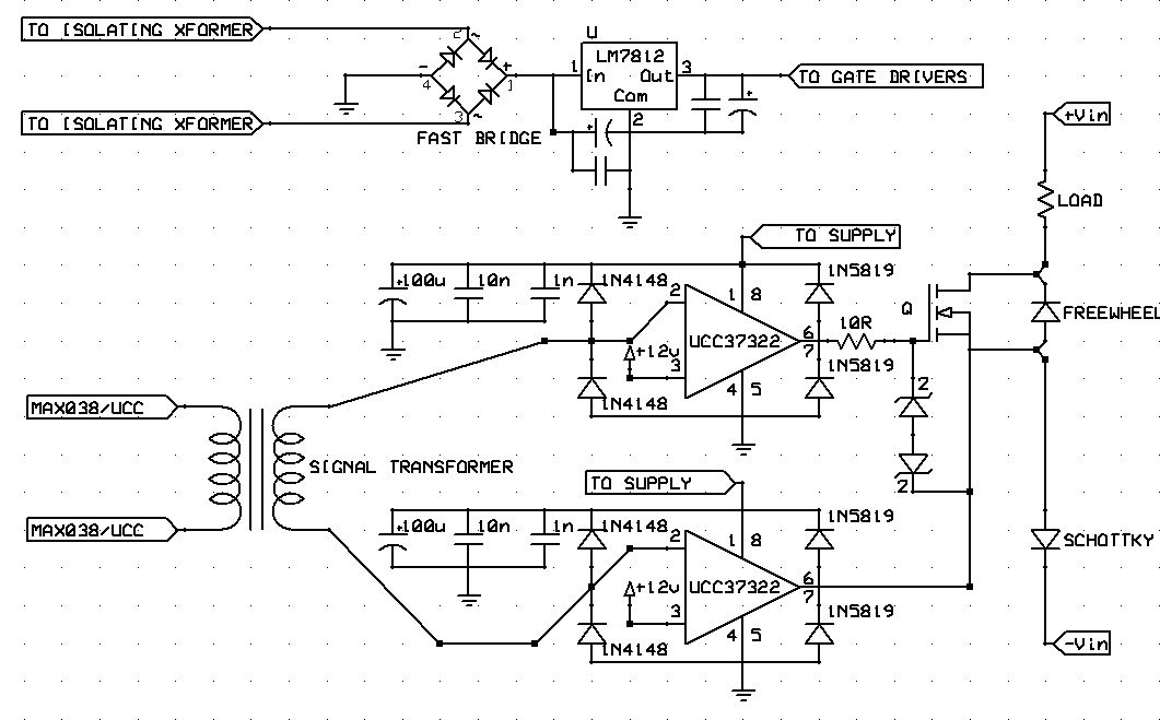
at the extreme right are four ultrafast diodes, a smoothing cap, then an LM7815 voltage regulator. This lil bridge is for rectifying a winding off a HF supply I haven't designed yet; this is where the board draws its isolated 15V supply from.
Underneath the regulator on the right you'll see a 100-ohm resistor, a schottky, and the apparent "signal in" connections. An isolated signal (e.g. from an oscillator) from another multifilar isolating transformer is connected between ground and the schottky. The schottky ensures the input pin of the UCCs don't cop a negative voltage, and the 100-ohm resistor allows the input capacitance to discharge so the things can turn off again.
Next you'll notice a complimentary pair of gatedrivers in an unusual configuration. The bottom one (UCC**) has had all its pins tortured around upside down such that when I socket the chip, I have effectively mirrored the left/right pinouts. This allows me to have a very neat layout for the inputs/outputs of the chip. Yes, I mean the legs are bent 180-degrees so you can see the underside of the chip when inserted.

You can see provisions for power bypass capacitors to the right of each chip; electrolytic, monolithic, and ceramic, each.
The top chip's output goes to an optional bank of DC blocking capacitors (which will probably be shorted out by a jumper), then to the source of the FET.
The bottom chip's output goes through a 10-ohm resistor to the gate of the FET. There's a TO220 freewheeling diode in there for the fun of it, too.
Out the bottom left of the board is a handy connection to the FET's drain. Out the top left, similarly, is a big pad for its source.
I'm hoping to push a bridge fairly hard with this setup, hence individual drivers for each transistor. Yes, I have to make four of these boards.
I'm looking for feedback on the board layout, and this isolated drive concept in general... =)
What do youse think?
Matt
Re: isolated gate drives
..., Wed May 10 2006, 04:27AM
No comments?
I will admit that it is considerably more complicated than a strait gdt, but whatever floats your boat...
For the minimal cost of making these, even if they each save one fet they are worth building...
Hmm, maybe you should add over current shutoff... Seems pretty easy, just put a very small sense resistor in series with low side of the fet and hook it up to the enable of the ucc Add a mov and you would have created an invincible switch
..., Wed May 10 2006, 04:27AM
No comments?
I will admit that it is considerably more complicated than a strait gdt, but whatever floats your boat...
For the minimal cost of making these, even if they each save one fet they are worth building...
Hmm, maybe you should add over current shutoff... Seems pretty easy, just put a very small sense resistor in series with low side of the fet and hook it up to the enable of the ucc
Add a mov and you would have created an invincible switch Re: isolated gate drives
ragnar, Thu May 11 2006, 08:24AM
as opposed to floating my mosfet's gate... =D
First problem I can see with my own board is that the connections on the edge for power and mosfet drain/source are actually outside the line projected by the edge of the MOSFET package, which means I can't stack four drives in a row with the FETs real close on the heatsink.
MUR860s might also not be the ideal diode packages - should I make provision for double-diode packages or diodes in series with the FET (to isolate the body diode)?? hrmmm
ragnar, Thu May 11 2006, 08:24AM
... wrote ...
...but whatever floats your boat...
...but whatever floats your boat...
as opposed to floating my mosfet's gate... =D
First problem I can see with my own board is that the connections on the edge for power and mosfet drain/source are actually outside the line projected by the edge of the MOSFET package, which means I can't stack four drives in a row with the FETs real close on the heatsink.
MUR860s might also not be the ideal diode packages - should I make provision for double-diode packages or diodes in series with the FET (to isolate the body diode)?? hrmmm
Re: isolated gate drives
Desmogod, Thu May 11 2006, 08:26AM
Considering that you run a PLL, is there any real need for the MUR's at all?
Desmogod, Thu May 11 2006, 08:26AM
Considering that you run a PLL, is there any real need for the MUR's at all?
Re: isolated gate drives
ragnar, Thu May 11 2006, 10:31AM
First, this isn't copping a PLL VCO, it's copping a MAX038 VCO (which does have an internal phase detector, but meh)... AND there's deadtime, AND there's signal modulation... so those diodes definitely have to freewheel =P
So, how do you like the layout and the idea of isolating the FETdrives at the power stage instead of output, to get that "hard" push/pull feel? =P
Re: isolated gate drives
Steve Conner, Thu May 11 2006, 10:41AM
As far as I know, the MURs are pointless unless you also have a schottky in series with the MOSFET, to make sure the body-drain diode gets isolated. I once did some experiments where I put a fast diode in parallel with a MOSFET's body-drain diode to see how the current shared between them. The fast diode had a higher forward voltage on account of being optimised for speed, so the body-drain diode ended up still passing all the current anyway.
Admittedly I used a 1200V fast diode (RURG30120) and 600V MOSFET (IRFP460) so the comparison may have been unfair. Some high voltage fast diodes can be two diodes in series internally.
Re: isolated gate drives
ragnar, Thu May 11 2006, 10:56AM
Eek, my MURs have a forward-voltage drop of ~0.4V, which will rise in duty, so I'll make that schottky a must... I scored some absolutely awesome 15A and 30A 60V schottkies off a laser printer board, but if this is running rectified mains, high voltage schottkies are expensive...
By the way, I just re-read the UCC datasheet, and on the ENBL pin they're happy down to -0.3V, and on the IN pin they're happy from -5V to VDD+0.3V.. so I can actually use a signal transformer without a 100-ohm resistor and schottky etc, so long as I've got an appropriate reduction down to +/-5V.. that makes things a lot neater and much more elegant, and just significantly changed my layout
I should also make provision for connecting that enable pin to something in the event that I actually decide to use it =)
So far I've fixed:
#1. input/output pads too close to board,
#2. allowing TO-247 double-diode packages to fit,
#3. making space for body-diode-isolating schottkies,
#4. removing the 100R and schottky on IN since it can take negative voltages,
Please, critique the crap out of my board. I didn't just put it here for flattery or to confuse y'all
ragnar, Thu May 11 2006, 10:56AM
wrote ...
As far as I know, the MURs are pointless unless you also have a schottky in series with the MOSFET, to make sure the body-drain diode gets isolated.
As far as I know, the MURs are pointless unless you also have a schottky in series with the MOSFET, to make sure the body-drain diode gets isolated.
Eek, my MURs have a forward-voltage drop of ~0.4V, which will rise in duty, so I'll make that schottky a must... I scored some absolutely awesome 15A and 30A 60V schottkies off a laser printer board, but if this is running rectified mains, high voltage schottkies are expensive...
By the way, I just re-read the UCC datasheet, and on the ENBL pin they're happy down to -0.3V, and on the IN pin they're happy from -5V to VDD+0.3V.. so I can actually use a signal transformer without a 100-ohm resistor and schottky etc, so long as I've got an appropriate reduction down to +/-5V.. that makes things a lot neater and much more elegant, and just significantly changed my layout
I should also make provision for connecting that enable pin to something in the event that I actually decide to use it =)
So far I've fixed:
#1. input/output pads too close to board,
#2. allowing TO-247 double-diode packages to fit,
#3. making space for body-diode-isolating schottkies,
#4. removing the 100R and schottky on IN since it can take negative voltages,
Please, critique the crap out of my board. I didn't just put it here for flattery or to confuse y'all
Re: isolated gate drives
Steve Conner, Thu May 11 2006, 12:22PM
The schottkies don't need to have a voltage rating equal to the supply voltage. 30v ones will do just fine, in fact they don't make high voltage schottkies (except for the mythical silicon carbide ones)
Steve Conner, Thu May 11 2006, 12:22PM
The schottkies don't need to have a voltage rating equal to the supply voltage. 30v ones will do just fine, in fact they don't make high voltage schottkies (except for the mythical silicon carbide ones)
Re: isolated gate drives
HV Enthusiast, Thu May 11 2006, 01:42PM
Actually, they do. I happen to have some 1500V Schottky diodes right here on my desk in front of me. And they
aren't SiC either . . .
HV Enthusiast, Thu May 11 2006, 01:42PM
wrote ...
in fact they don't make high voltage schottkies (except for the mythical silicon carbide ones
in fact they don't make high voltage schottkies (except for the mythical silicon carbide ones
Actually, they do. I happen to have some 1500V Schottky diodes right here on my desk in front of me. And they
aren't SiC either . . .
Re: isolated gate drives
ragnar, Thu May 11 2006, 01:52PM
Hey, EVR, good to see someone looking at my lonely lil thread here.
Perhaps you could utter a few words of guidance regarding my [strange] ideas... ^^
ragnar, Thu May 11 2006, 01:52PM
Hey, EVR, good to see someone looking at my lonely lil thread here.
Perhaps you could utter a few words of guidance regarding my [strange] ideas... ^^
Re: isolated gate drives
HV Enthusiast, Thu May 11 2006, 03:05PM
Do you have a schematic to post???
HV Enthusiast, Thu May 11 2006, 03:05PM
blackplasma wrote ...
Hey, EVR, good to see someone looking at my lonely lil thread here.
Perhaps you could utter a few words of guidance regarding my [strange] ideas... ^^
Hey, EVR, good to see someone looking at my lonely lil thread here.
Perhaps you could utter a few words of guidance regarding my [strange] ideas... ^^
Do you have a schematic to post???
Re: isolated gate drives
Steve Conner, Thu May 11 2006, 03:57PM
OMG, EVR, are they diamond? Or kryptonite?
Steve Conner, Thu May 11 2006, 03:57PM
OMG, EVR, are they diamond? Or kryptonite?
Re: isolated gate drives
Marko, Thu May 11 2006, 04:55PM
As I could figure out reverse voltage is the main reason why schottkyes haven't pwned 'ordinary' diodes yet. For what I know 600V is the highest voltae silicon-carbide diodes acheived, and these still seeh relatively hard to get, and they don't have some great current rating (about 12A at most)
Re: isolated gate drives
HV Enthusiast, Thu May 11 2006, 06:15PM
They are diamond based. And basically they are prototypes only provided to us for an R&D effort we are working on.
HV Enthusiast, Thu May 11 2006, 06:15PM
They are diamond based. And basically they are prototypes only provided to us for an R&D effort we are working on.
Re: isolated gate drives
Wilson, Fri May 12 2006, 09:05AM
There seems to be a small error in regards to the schottky/freewheel section on your schem.
The schottky in series with the source of the FET is supposed to have its cathode connected to the anode of the freewheeling diode
Effectively, what you've just done is to isolate both the body diode AND the freewheeling one using the schottky, meaning that something will probably so pop or smoke when you get reverse current
Anyways, using an independant gate driver for each FET isn't quite a bad idea. You can drive the gates alot harder, and makes paralleling mosfets a more feasible idea.
Keep up the good work
Wilson
Re: isolated gate drives
Steve Conner, Fri May 12 2006, 10:13AM
Ya, Wilson is right. You should also have at least one pull-down resistor connected across one of those 1N4148s. I would tend to put one ~470 ohm resistor from each UCC input to ground. It's just to stop the transformer winding floating around.

I found this on Obi-Wan Burnett's site
Steve Conner, Fri May 12 2006, 10:13AM
Ya, Wilson is right. You should also have at least one pull-down resistor connected across one of those 1N4148s. I would tend to put one ~470 ohm resistor from each UCC input to ground. It's just to stop the transformer winding floating around.
I found this on Obi-Wan Burnett's site
Re: isolated gate drives
ragnar, Fri May 12 2006, 03:11PM
Ah yes, schottky/body diode etc... OOPS on my part.
I'm getting the general impression from the datasheet that I should have my low-impedance/bypass caps on the output side of the UCC...
I'l considering sacrificing my principles and placing them "across" the output rail on pin6/7...
Should be relatively neat.
Re: isolated gate drives
Part Scavenger, Sun May 14 2006, 02:04AM
One problem. I don't see an audiomodulation circuit.
Looks pretty cool, and the layout is just sexy!
Part Scavenger, Sun May 14 2006, 02:04AM
One problem. I don't see an audiomodulation circuit.
Looks pretty cool, and the layout is just sexy!
Re: isolated gate drives
ragnar, Wed May 17 2006, 10:17AM
I seemed to have had this board all perfect and nice, but had to mangle it by fitting that power schottky in there (to bypass the FET's body-diode)...
I've taken the zeners off the board because they were a PITA, and it's reasonably easy to clip them onto the MOSFET nice and close/directly. The gate resistor now has to go under the board because of the schottky being in the way. I'm not happy with the enclosed loop area between OUT1/SOURCE/GATE/OUT2, but it'll do.
I've got Steve-Conner-memorial schottkies on the outputs of both UCCs, and signal diodes on the inputs to clamp my +/-5V signal just in case it rings to something silly, and a 1K pulldown on each UCC input.
I've also put the power bypass caps on the output side of the chip and thickened up the MOSFET and DIODE and SCHOTTKY tracks.
I've got the UCCX732X datasheet here, and they're available in DIP8, SOIC8 and MSOP8... and funnily enough, the MSOP8 has a power dissipation rating almost 3 times that of DIP8 (1370mW versus
500mW)... it also has a C/W temp rating better than 10 times that of the DIP, when properly soldered down on its tinned thermal pad.
It's very tempting... USD$54 for 25ea of the MSOP UCC27322s (yes, TWO-7322 is rated for higher die temperatures than the 37322)...
They (the MSOP packages) would also be a much better fit when it comes to snuggling up to the FETs regarding loop area...
Has anyone got experience with the MSOP UCCs? Please rant here!
Any overhauls I should make to the layout before committing?
-Matt =)
Thanks mod, I forgot GIF's aren't resized.
Re: isolated gate drives
Avalanche, Wed May 17 2006, 11:04AM
To get your isolated power supplies for each driver, couldn't you use a big capacitive divider (with say 4 caps) and feed it with 100v+? I haven't thought this through properly but the thought just popped into my head...
Avalanche, Wed May 17 2006, 11:04AM
To get your isolated power supplies for each driver, couldn't you use a big capacitive divider (with say 4 caps) and feed it with 100v+? I haven't thought this through properly but the thought just popped into my head...
Re: isolated gate drives
ragnar, Wed May 17 2006, 10:17PM
A capacitive divider is an interesting idea for AC, but I feel the distributed power / isolation transformer is more appropriate for varying input voltages, etc =)
Surely, EVR, you've worked with MSOP powerpad packages? (With the ground/die exposed at the bottom of the chip, which you reflow solder to the board to take heat away? =)
Re: isolated gate drives
..., Wed May 17 2006, 10:58PM
I have never worked with said packages, but in the one board I have made...
I had a voltage regulator in a little package which I needed to dissipate a little over a watt with, so I just put about 1cm by .5cm copper area on the tab and put a few vias (hole with piece of wire soldered on either side) around it into a similar sized piece of copper on the back. It seemed to work just fine, both sides got equally as warm...
I would say for these chips you should use a H shaped copper fill so you have tabs on either side of the chips, and from put a bunch of pins through to the bottom of the board... I suppose if you wanted to keep the flat format of your boards you could use some copper foil on either side to get the heat down to the bottom of the board.
As to the supply... I would have to say the best method would be to use a little ferrite core powered by a mazzilli driver or just a simple fixed frequency oscillator... Then wind a secondary for each board and have fun. Even normal magnet wire should be able to handle the <500v that would ever be across the bridge...
Re: isolated gate drives
HV Enthusiast, Wed May 17 2006, 11:11PM
Yes, I have worked with MSOPs, although i never hand soldered them. They would definitely be an improvement over DIP packages as with a DIP package, the only heat path is through the pins themselves which is pretty poor.
HV Enthusiast, Wed May 17 2006, 11:11PM
Yes, I have worked with MSOPs, although i never hand soldered them. They would definitely be an improvement over DIP packages as with a DIP package, the only heat path is through the pins themselves which is pretty poor.
Re: isolated gate drives
ragnar, Wed May 17 2006, 11:16PM
Steve Conner used a ZVS as the sinewave wouldn't induce as much noise as sharp squarewaves... IIRC. I'll be doing something similar, it's the best way.
Now I don't have to execute my "UCCs under oil" plan =P
ragnar, Wed May 17 2006, 11:16PM
Steve Conner used a ZVS as the sinewave wouldn't induce as much noise as sharp squarewaves... IIRC. I'll be doing something similar, it's the best way.
Now I don't have to execute my "UCCs under oil" plan =P
Re: isolated gate drives
Steve Conner, Thu May 18 2006, 09:07AM
That's exactly what I'm using for my isolated gate drivers, the Mazzilli oscillator circuit. I wanted sine waves for quite a long and complicated reason.
I designed my isolated drivers as four drive boards that mount very close to their IGBTs, and plug into the main PLL box with Cat5 network cables. So I had to feed the HF AC power down this cable along with the gate drive signal. I thought if I used a square wave, the edges might couple capacitively over into the gate drive signal.
In practice I found that when I rectify the sine wave on the gate driver board, the diode recovery spikes add lots of crud anyway. But the Mazzilli circuit is real nice and simple. I found that if I used a choke input filter on the rectifier, the voltage regulation was good enough that I could get away without regulator ICs on each board. I just used a zener to draw some current, since the voltage skyrockets if you draw less than a critical value.
I used a ferrite E core with airgap for the mazzilli circuit, with a single output winding that fed a little ferrite toroid 1:1 isolating transformer on each board. I just did that so the different cores on the Cat5 cable wouldn't have high voltages between them. If you wanted to save some hassle, it should be fine to combine the oscillator and isolation transformer into a single component with 5 windings, the way Steve Ward etc. did. Just make sure you remember what is grounded and what is floating on your DC bus voltage.
I haven't time to think through the capacitive divider thing that Avalanche mentioned, but it just sounds plain wrong. :(
Steve Conner, Thu May 18 2006, 09:07AM
That's exactly what I'm using for my isolated gate drivers, the Mazzilli oscillator circuit. I wanted sine waves for quite a long and complicated reason.
I designed my isolated drivers as four drive boards that mount very close to their IGBTs, and plug into the main PLL box with Cat5 network cables. So I had to feed the HF AC power down this cable along with the gate drive signal. I thought if I used a square wave, the edges might couple capacitively over into the gate drive signal.
In practice I found that when I rectify the sine wave on the gate driver board, the diode recovery spikes add lots of crud anyway.
But the Mazzilli circuit is real nice and simple. I found that if I used a choke input filter on the rectifier, the voltage regulation was good enough that I could get away without regulator ICs on each board. I just used a zener to draw some current, since the voltage skyrockets if you draw less than a critical value.I used a ferrite E core with airgap for the mazzilli circuit, with a single output winding that fed a little ferrite toroid 1:1 isolating transformer on each board. I just did that so the different cores on the Cat5 cable wouldn't have high voltages between them. If you wanted to save some hassle, it should be fine to combine the oscillator and isolation transformer into a single component with 5 windings, the way Steve Ward etc. did. Just make sure you remember what is grounded and what is floating on your DC bus voltage.
I haven't time to think through the capacitive divider thing that Avalanche mentioned, but it just sounds plain wrong. :(
Re: isolated gate drives
Marko, Thu May 18 2006, 05:08PM
Wouldn't it be simplest to use one transformer like steve ward's big DRSSTC (a bunch of CAT5 wrapped around flyback core), possibly rectified at the place and fed to each driver?
Marko, Thu May 18 2006, 05:08PM
Wouldn't it be simplest to use one transformer like steve ward's big DRSSTC (a bunch of CAT5 wrapped around flyback core), possibly rectified at the place and fed to each driver?
Re: isolated gate drives
Desmogod, Fri May 19 2006, 07:46AM
I think you are missing the point of the exercise.
Desmogod, Fri May 19 2006, 07:46AM
Firkragg wrote ...
Wouldn't it be simplest to use one transformer like steve ward's big DRSSTC (a bunch of CAT5 wrapped around flyback core), possibly rectified at the place and fed to each driver?
Wouldn't it be simplest to use one transformer like steve ward's big DRSSTC (a bunch of CAT5 wrapped around flyback core), possibly rectified at the place and fed to each driver?
I think you are missing the point of the exercise.
Re: isolated gate drives
ragnar, Sat May 20 2006, 02:38PM
It was a dark and stormy night... the rain fell in torrents...except at occasional intervals, when it was checked by a violent gust of wind which swept up the streets (for it is in Sydney that our scene lies), rattling along the housetops, and fiercely agitating the blue glow of the fluorescent lamps that struggled against the darkness...
And deep in the laboratory... I started pulling isolated-gate-driver circuit boards out of my arse.
The 'ghosting (pun intended)' you see is from the nosecone rubbing oil over the surface of the board as it engraves.


Re: isolated gate drives
ragnar, Sun May 21 2006, 10:39AM
OK, since none of you buggers replied to my prose... I'm going to... post more pictures. (These ones are better lit since I wasn't working at midnight)
Boards had until now been conceived, designed, flipped, engraved.
Today I drilled all holes (73 holes per board, a total of 730 holes over ten boards) using 0.8mm solid tungsten carbide drills by UNION TOOL, which performed very well after I biased the axial slop in my cheap drill press to the left with an ockey strap.
These were previously 3oz double sided copper boards. I'd removed one side of the copper by peeling. Now with my excellent co-ordination since they were separated, I weeded out the groundplane from all boards (since there were artefacts from engraving, copper shavings and whiskers, and general distance issues etc) so it's now just the copper tracks.
Now I ground all ten boards' edges to size, gave them a quick acetone clean, and they are ready for tinning! =)
Stuffing will be the fun part, because then I can see how my isodrives actually perform!
Comments?


Re: isolated gate drives
Wilson, Sun May 21 2006, 01:46PM
sweet stuff~ Hope it works as good as it looks. Show those stubborn FETs what your're made out of.
btw, just curious, but doesn't having too high a peak current on the gate actually damage the oxide layer?
Wilson, Sun May 21 2006, 01:46PM
sweet stuff~ Hope it works as good as it looks. Show those stubborn FETs what your're made out of.
btw, just curious, but doesn't having too high a peak current on the gate actually damage the oxide layer?
Re: isolated gate drives
ragnar, Sun May 21 2006, 03:11PM
Yes, brutalizing the gate will damage a FET. The point of this driver it so minimise any inductive ringing between the drivers and the FET. Since the transistor(s) will be in zcs/zvs situations, I don't think the gate current need be too big... There's also provision underneath the board for a gate resistor.
------ Mod edit combined double post -------
Quiet in here...
so I assembled one of the boards (with the exception of the green screwterminals, which I'm out of, and wouldn't fit anyway as I have to enlarge the holes)... it's reasonably pretty in its own right =)
If you look at the third pic, the gold pins on the left is where AC (from isolating ferrite) is dropped in. The next set of PCB pins is where an isolated drive signal is connected. The top right PCB pin is where you'd connect the FET's drain, the bottom right PCB pin is where you'd connect the FET's source.
That's a fake schottky standing up on the right, too.
NOW will you guys comment? And tell me I haven't got my board back-to-front or anything.... especially considering I just made ten.


Re: isolated gate drives
Steve Conner, Sun May 21 2006, 03:48PM
Oi!!!! You're breaking the double posting rule. *bitch slap*
Apart from that, your drive boards look great. I'm mighty impressed by the CNC engraving.
Steve Conner, Sun May 21 2006, 03:48PM
Oi!!!! You're breaking the double posting rule. *bitch slap*
Apart from that, your drive boards look great. I'm mighty impressed by the CNC engraving.
Re: isolated gate drives
..., Sun May 21 2006, 07:12PM
Wow, bp made a though hole board
Looking good, lets see them put to work... I want to see the anticoil going...
I found it kind of odd that you separated them all, seems like it would be easier to leave them in banks of 4 to keep the fets organized... You could have even left a little strip on the bottom of the board to mount the transformers and even the driver on to keep everything organised... Oh well
I think you had all the right to make that double post...
Re: isolated gate drives
Part Scavenger, Mon May 22 2006, 11:48AM
Looks great BP! Top quality as usual.
Part Scavenger, Mon May 22 2006, 11:48AM
Looks great BP! Top quality as usual.
Re: isolated gate drives
Adam Horden, Tue May 23 2006, 11:08AM
Steve,
You talk about it capacitlvey coupling to the gate drive signal from the HF AC supply. I would probally be more considrdned with crosstalk. When the coil is running you could get all sorts of noise that could be coulded capacitvley and electromagnetic onto the gate drive signal.
But if you use the foil twisted pair CAT5 cable you also get a good screen thrown in and there not to expensive. It was one of the methods I was going to use to drive my CM600s but I opted to sue BNC cables and BNC connectors in the finish.
Adam
Adam Horden, Tue May 23 2006, 11:08AM
Steve Conner wrote ...
That's exactly what I'm using for my isolated gate drivers, the Mazzilli oscillator circuit. I wanted sine waves for quite a long and complicated reason.
I designed my isolated drivers as four drive boards that mount very close to their IGBTs, and plug into the main PLL box with Cat5 network cables. So I had to feed the HF AC power down this cable along with the gate drive signal. I thought if I used a square wave, the edges might couple capacitively over into the gate drive signal.
In practice I found that when I rectify the sine wave on the gate driver board, the diode recovery spikes add lots of crud anyway. But the Mazzilli circuit is real nice and simple. I found that if I used a choke input filter on the rectifier, the voltage regulation was good enough that I could get away without regulator ICs on each board. I just used a zener to draw some current, since the voltage skyrockets if you draw less than a critical value.
I used a ferrite E core with airgap for the mazzilli circuit, with a single output winding that fed a little ferrite toroid 1:1 isolating transformer on each board. I just did that so the different cores on the Cat5 cable wouldn't have high voltages between them. If you wanted to save some hassle, it should be fine to combine the oscillator and isolation transformer into a single component with 5 windings, the way Steve Ward etc. did. Just make sure you remember what is grounded and what is floating on your DC bus voltage.
I haven't time to think through the capacitive divider thing that Avalanche mentioned, but it just sounds plain wrong. :(
That's exactly what I'm using for my isolated gate drivers, the Mazzilli oscillator circuit. I wanted sine waves for quite a long and complicated reason.
I designed my isolated drivers as four drive boards that mount very close to their IGBTs, and plug into the main PLL box with Cat5 network cables. So I had to feed the HF AC power down this cable along with the gate drive signal. I thought if I used a square wave, the edges might couple capacitively over into the gate drive signal.
In practice I found that when I rectify the sine wave on the gate driver board, the diode recovery spikes add lots of crud anyway.
But the Mazzilli circuit is real nice and simple. I found that if I used a choke input filter on the rectifier, the voltage regulation was good enough that I could get away without regulator ICs on each board. I just used a zener to draw some current, since the voltage skyrockets if you draw less than a critical value.I used a ferrite E core with airgap for the mazzilli circuit, with a single output winding that fed a little ferrite toroid 1:1 isolating transformer on each board. I just did that so the different cores on the Cat5 cable wouldn't have high voltages between them. If you wanted to save some hassle, it should be fine to combine the oscillator and isolation transformer into a single component with 5 windings, the way Steve Ward etc. did. Just make sure you remember what is grounded and what is floating on your DC bus voltage.
I haven't time to think through the capacitive divider thing that Avalanche mentioned, but it just sounds plain wrong. :(
Steve,
You talk about it capacitlvey coupling to the gate drive signal from the HF AC supply. I would probally be more considrdned with crosstalk. When the coil is running you could get all sorts of noise that could be coulded capacitvley and electromagnetic onto the gate drive signal.
But if you use the foil twisted pair CAT5 cable you also get a good screen thrown in and there not to expensive. It was one of the methods I was going to use to drive my CM600s but I opted to sue BNC cables and BNC connectors in the finish.
Adam
Re: isolated gate drives
ragnar, Sun Jun 25 2006, 01:37AM
Hi all,
although it's taken in excess of a month, I've done several revisions on the power supply, signal circuitry, and actual isodriver circuits. It's (tentatively) working (the power, at least), and I'll assemble some other boards and see if it'll swing a FET!
I also built a cute little current-limited (with electrolytics, don't ask!) power supply, which has greatly reduced the number of silicon fatalities during development to just a few diodes! =)
So what y'all think?


Re: isolated gate drives
..., Sun Jun 25 2006, 02:01AM
I think they look great I also hope that the boards you are (or are not?) making for me look as good
In any case, what is the upper waveform on the scope? My best guess is that the lower trace is across the output of one of the isolated outputs from the zvs powered isolation transformer, but I hope the top trace isn't the gate drive Put a zener or something on that...
..., Sun Jun 25 2006, 02:01AM
I think they look great
I also hope that the boards you are (or are not?) making for me look as good In any case, what is the upper waveform on the scope? My best guess is that the lower trace is across the output of one of the isolated outputs from the zvs powered isolation transformer, but I hope the top trace isn't the gate drive
Put a zener or something on that...Re: isolated gate drives
Steve Conner, Sun Jun 25 2006, 01:23PM
Yea, something looks not right with those waveforms. :-/ Here's what mine look like:
Top trace is gate voltage @ 10V/div
Middle trace is drain voltage of same FET @ 50V/div
Bottom trace is output from transformer @ 50V/div

I'm running off 21V DC and producing about 30V RMS output. The transformer secondary is centre tapped to ground, so you only see half the output voltage on the scope.
Re: isolated gate drives
ragnar, Mon Jun 26 2006, 02:59AM
Well, fine.
I f1x0r3d mine by reducing the gate resistors to 100-ohms each, adding some more inductance to my choke, replacing the overkill IRFP450s with IRF540Ns, and changing the resonant capacitor to 100nF.
Ha!
And the sinewave isn't perfect, because it was loaded down very badly by a 16V electrolytic on one of my power supply boards (oops) which promptly exploded after I took the photo, the gush of electrolyte gas narrowly missing my eye


Re: isolated gate drives
..., Mon Jun 26 2006, 06:05AM
ah, much better
Lets seem some gate waveforms on the big fets! Or even better some sparks!
..., Mon Jun 26 2006, 06:05AM
ah, much better
Lets seem some gate waveforms on the big fets! Or even better some sparks!
Re: isolated gate drives
teravolt, Wed Jun 28 2006, 04:07AM
at presant I'm working on a pcb that is simular to yours but I'm using FRED diods RURG80100 that have I belive a 55nS recovery time in the configuration that Steave Conner illistrated. I also included a opto isolator in front of the drivers for galvonic isolation for foalting purpases.
Re: isolated gate drives
ragnar, Thu Jun 29 2006, 03:46AM
Weee, swinging a small FET gate at 2.2MHz... now to get onto the bigger stuff... where's my signal generator? heheh
Because of my paranoia (and lack of cash), I did isolation by ferrite instead of optoisolation. For the digital signals though, optos are probably the way to go... hehe.. next time! =D
no sparks yet... I just realised I forgot the leakage resistors (1K) on the gatedriver inputs, so I have to add those underneath to the four boards before they'll do anything. There's not enough leakage through IN for a bipolar signal to trigger them. Meh.


Re: isolated gate drives
..., Thu Jun 29 2006, 04:04AM
Those spikes are a little big, but so long as you aren't exceeding the max voltage of the gates you should be ok... You did put zeners on the gates, right?
Looks good in any case!
..., Thu Jun 29 2006, 04:04AM
Those spikes are a little big, but so long as you aren't exceeding the max voltage of the gates you should be ok... You did put zeners on the gates, right?
Looks good in any case!
Re: isolated gate drives
ragnar, Thu Jun 29 2006, 04:31AM
Top waveform is the 5Vp/p signal from the signal generator going to ferrite (isolation) to the isodriver board, the bottom waveform is the voltage across the FET. There are no zeners on the gates, since the gatedrivers are clamped to the rails with diodes, and there is no isolation between the FETs and gatedrivers.
I'm using 10-ohm gate resistors atm, but to square up the waveforms (since the drivers really can provide the current) I'm considering 1-3 ohm.
Here's the circuit driving a bigger FET, (IRFP450) at 2.4MHz


Re: isolated gate drives
Steve Conner, Thu Jun 29 2006, 09:20AM
Nice work BP! Driving a big power FET at 2.4MHz isn't that easy, especially while keeping HV isolation, but you seem to have pulled it off in style. Time to stick some DC bus voltage up it and check for common-mode noise immunity now.
Steve Conner, Thu Jun 29 2006, 09:20AM
Nice work BP!
Driving a big power FET at 2.4MHz isn't that easy, especially while keeping HV isolation, but you seem to have pulled it off in style. Time to stick some DC bus voltage up it and check for common-mode noise immunity now.Re: isolated gate drives
Marko, Thu Jun 29 2006, 12:03PM
I don't know if this is a good idea but could a DC blocking capacitor (big) in series with FET gate be an additional safety?
When MOSFET dies he usually connects 'all pins together' attempting to fry more parts in the circuit.
Then in some occasions mosfet's source pin may blow open and leave DC bus supply voltage on your gate driver resulting in spectacular death of drivers.
Cap would just 'charge up' and current will be unable to flow anymore.
It would have to be combined with TVS or stronger zenerson UCC's output to survive initial 'shock'.
(???)
Spikes are quite normal whebn drving FET directly with gate drivers. Higher current gate drivers usually make bigger spikes.
Yeah, but I would like to see gate waveform! =)
From just input oscillatr signal and FET voltage (voltage across MOSFET always looks wierd like that ).
Marko, Thu Jun 29 2006, 12:03PM
I don't know if this is a good idea but could a DC blocking capacitor (big) in series with FET gate be an additional safety?
When MOSFET dies he usually connects 'all pins together' attempting to fry more parts in the circuit.
Then in some occasions mosfet's source pin may blow open and leave DC bus supply voltage on your gate driver resulting in spectacular death of drivers.
Cap would just 'charge up' and current will be unable to flow anymore.
It would have to be combined with TVS or stronger zenerson UCC's output to survive initial 'shock'.
(???)
Those spikes are a little big, but so long as you aren't exceeding the max voltage of the gates you should be ok... You did put zeners on the gates, right?
Spikes are quite normal whebn drving FET directly with gate drivers. Higher current gate drivers usually make bigger spikes.
Top waveform is the 5Vp/p signal from the signal generator going to ferrite (isolation) to the isodriver board, the bottom waveform is the voltage across the FET. There are no zeners on the gates, since the gatedrivers are clamped to the rails with diodes, and there is no isolation between the FETs and gatedrivers.
Yeah, but I would like to see gate waveform! =)
From just input oscillatr signal and FET voltage (voltage across MOSFET always looks wierd like that ).
Re: isolated gate drives
ragnar, Thu Jun 29 2006, 12:47PM
Aw thanks Steve, I'm chuffed =)
Firkragg, the bottom waveform is the (gate) voltage across the FET. My apologies for the ambuguity =P
On this image:

The top waveform is the 5Vp/p signal going into the gatedriver.
The bottom waveform is the gate voltage of a random TO-220 FET at 2.2MHz (mind you with a 10-ohm series gate resistor, making the edges very curvy).
On this image:

Similarly, the top waveform is a 5Vp/p signal going into the gatedriver (hysteresis is 2V on, 1V off).
The bottom waveform is the gate of an IRFP450 FET at 2.4MHz. I need to lower the gate resistor more because the switching times are a little slow.
Better now?
ragnar, Thu Jun 29 2006, 12:47PM
Aw thanks Steve, I'm chuffed =)
Firkragg, the bottom waveform is the (gate) voltage across the FET. My apologies for the ambuguity =P
On this image:
The top waveform is the 5Vp/p signal going into the gatedriver.
The bottom waveform is the gate voltage of a random TO-220 FET at 2.2MHz (mind you with a 10-ohm series gate resistor, making the edges very curvy).
On this image:
Similarly, the top waveform is a 5Vp/p signal going into the gatedriver (hysteresis is 2V on, 1V off).
The bottom waveform is the gate of an IRFP450 FET at 2.4MHz. I need to lower the gate resistor more because the switching times are a little slow.
Better now?
Re: isolated gate drives
ragnar, Fri Jun 30 2006, 01:33AM
This morning i've bolted down all eight packages to a heatsink (precariously), and fired up all the isodrivers at once, with the correct combination of inverting/noninverting chips =P
my power supply is struggling a little (just vibrating a wee bit), but not below the dropout voltage of any of the regulators.
there's sinewavey noise on the signals, regardless of the frequency, which I can see with the timebase on my scope set to fastest and the intensity at brightest... but there's nothing I'm running at that frequency, so must be parasitic ringing from elsewhere.
All the drivers seem to work the same, however I'm curious as to what the little artefact is just prior to the turn-off transition on each pulse... hmmm


Re: isolated gate drives
..., Fri Jun 30 2006, 02:35AM
I really worry about that sign wave on the gate waveforms... If those are real you have serous problems
In any case, me like! But I want to see that anticoil primary you made working!
..., Fri Jun 30 2006, 02:35AM
I really worry about that sign wave on the gate waveforms... If those are real you have serous problems
In any case, me like! But I want to see that anticoil primary you made working!
Re: isolated gate drives
ragnar, Fri Jun 30 2006, 02:41AM
The fuzzy wavey noise disappears when I grab just about any component, including the scope's ground lead, so we'll see what happens.
ragnar, Fri Jun 30 2006, 02:41AM
The fuzzy wavey noise disappears when I grab just about any component, including the scope's ground lead, so we'll see what happens.
Re: isolated gate drives
Steve Ward, Fri Jun 30 2006, 04:47AM
You are coupling noise through the drains of each fet to the heatsink. You should find out how to remedy this before you cause your gate drivers to overheat! This is the common mode noise Conner mentioned. Luckily, my big IGBT brick drives dont seem to suffer from this despite not even considering the problem when i designed them.
Not really... high dissipation is to be expected at 2.4mhz with common fets. If he is careful about zero current switching with his load, then he should be fine.
Steve Ward, Fri Jun 30 2006, 04:47AM
You are coupling noise through the drains of each fet to the heatsink. You should find out how to remedy this before you cause your gate drivers to overheat! This is the common mode noise Conner mentioned. Luckily, my big IGBT brick drives dont seem to suffer from this despite not even considering the problem when i designed them.
If those are real you have serous problems
Not really... high dissipation is to be expected at 2.4mhz with common fets. If he is careful about zero current switching with his load, then he should be fine.
Re: isolated gate drives
Steve Conner, Fri Jun 30 2006, 09:47AM
That fuzzy ringy stuff looks like some sort of parasitic oscillation. If it were just ringing excited by the gate drive edges, it would have a decaying envelope. Anyway the acid test is when you connect those FETs to some power and see if the waveforms still look nice when everything is di/dt'ing and dv/dt'ing all over the place like crazy.
Good luck trying to get a low enough inductance layout to work at 2MHz, with your FETs in a row
Re: isolated gate drives
ragnar, Fri Jun 30 2006, 11:29AM
heheh, that wasn't just for photo mockup, but to test the drivers all at once (and consider switching a few volts through a resistor)... =P
I should have posted the pic of solid aluminium stock I'm using for separate heatsinks...
..hehe, now, how to have a low-inductance layout, but not have the plates parallel next to each other, forming an air capacitor... ^^
Print this page