
GaN Class E Coil
Weston, Tue Dec 13 2016, 06:53AMLoneoceans has first claim to a SiC coil, so I have decided to post my recent work on my GaN class E coil. The system runs at 6.78MHz.
My last set of class E plasma tweeters worked decently but had an issue with breakout on startup (or rather the lack of). Class E amplifiers are sensitive to load variations, and no breakout is a rather extreme case of that. It causes loss of zero voltage switching and the power FETs blow up in short order.
The research group I work in has a paper (
 ) on modifications to the class E topology where the DC feed inductor is also resonant, which significantly extends the range the resistive component of the load impedance can be without losing ZVS. This corresponds to zero voltage switching with a wide range loading from the plasma discharge (or lack of). I decided to model the RF amplifier for my nex plasma tweeters off this variation to the topology.
I also decided this would be a good test bed for the new GaN fets on the market. The GaN system fets look good for a class E coil but are a pain to heatsink like most of the GaN fets on the market. The 650V line looked good and I chose the 30A version because it was stocked by american distributors.

This coil is as much of a topology test as a thermal test. I am mounting the FETs on the underside of the PCB and clamping the entire PCB on top of a heatsink. The GaN fets have a tiny top side thermal pad connected to the source so I can use a graphite thermal pad to still get a thermal resistance between the junction and the heatsink of ~ 3 C/W.
I am trying to keep most of the work on this github page:

Today I got first light, about 150W in yields this discharge:
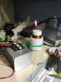
Right now, the transistors seem to stay cool, but the feed inductors start smoking. That implies that there is a much larger current flowing through them than I expected, which does not match my simulation. I guess the next step is figuring out that discrepancy.
Re: GaN Class E Coil
Steve Ward, Thu Dec 15 2016, 05:04AM
Cool! I've been thinking about playing with some 100V gan-fets for driving a HF coil. I see you used the STM32F334, what IDE did you use for compiling code? And did you utilize its high frequency timer/counter?
Steve Ward, Thu Dec 15 2016, 05:04AM
Cool! I've been thinking about playing with some 100V gan-fets for driving a HF coil. I see you used the STM32F334, what IDE did you use for compiling code? And did you utilize its high frequency timer/counter?
Re: GaN Class E Coil
Weston, Fri Dec 16 2016, 08:05AM
I use a basic text editor (sublime) with GCC for compile and OCD for jtag. Files for all that are on the github page. Right now the STM32F334 just generates 180 degree square waves for gate drive using the high resolution timer. My last full plasma tweeters used it for a class D modulator running at 400KHz, I just used the chip and my old code in this test setup for quick prototyping.
The 100V GaN fets would be good for class DE. Especially as the "body diode" of these devices has no reverse recovery loss. I considered trying class DE but I am trying to stay at 6.78MHz and high side gate drivers at that frequency are difficult.
I figured out the issue with the inductors. I misinterpreted the datasheet and did not realize skin effect was not included in the loss figures. I was getting ~10X the loss, so while I expected a 25C temp rise it was a ~ 250C temp rise. I wound some inductors out of rectangular magnet wire I had access to, but I did not like the aesthetic. I 3d printed a jig so I could wind the rectangular wire along the thick axis and wound some new inductors today. Still a bit clunky looking, but lower losses.
Since I was winding my own inductors I also increased the feed inductor value, which increases the impedance of the system. This will give me a better match to the on resistance / max voltage of the fets. The current board is limited to 100V input but with a safety margin I can run this GaN fets in class E up to 160V. Right now the system draws ~ 3A at 50V (150W). I need to get a higher voltage power supply for further testing and to see how much power I can push through this board.
I think a cool next step would be to take a better look at the class phi-2 topology. It adds an additional resonant network to reduce the voltage across the mosfet to ~ 2.5 the supply voltage when compared to ~3.2 (pi) times the supply voltage for class E. This should allow me to run the system directly off the AC line with a greater safety margin. Component selection is a bit more nuanced, but I will have to see if I can get it working in simulation over the winter break and spin another PCB.
I also thought a bit about protection of the class E power stage. Things can blow up quickly when the zero voltage switching is lost. The loss of ZVS implies that the waveform across the mosfet has changed from a half period of a sine wave to some smaller portion. As this waveform must integrate to the supply voltage (average voltage across an inductor is zero), I should be able to detect this condition by a decrease in the peak DS voltage. Similarly, I should be able to detect mistuning in the other direction (natural resonant frequency too high, leading to body diode conducting), by an increase in the peak DS voltage. This would allow me to monitor the system with a slow ADC.
Some more Photos:
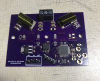
Close Up of the PCB
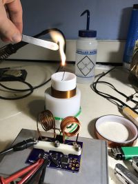
Drawing an arc of the secondary. For scale, the entire secondary is 5.5" tall.

Winding form to constrain the rectangular wire and allow me to wind it along the long axis.
Weston, Fri Dec 16 2016, 08:05AM
I use a basic text editor (sublime) with GCC for compile and OCD for jtag. Files for all that are on the github page. Right now the STM32F334 just generates 180 degree square waves for gate drive using the high resolution timer. My last full plasma tweeters used it for a class D modulator running at 400KHz, I just used the chip and my old code in this test setup for quick prototyping.
The 100V GaN fets would be good for class DE. Especially as the "body diode" of these devices has no reverse recovery loss. I considered trying class DE but I am trying to stay at 6.78MHz and high side gate drivers at that frequency are difficult.
I figured out the issue with the inductors. I misinterpreted the datasheet and did not realize skin effect was not included in the loss figures. I was getting ~10X the loss, so while I expected a 25C temp rise it was a ~ 250C temp rise. I wound some inductors out of rectangular magnet wire I had access to, but I did not like the aesthetic. I 3d printed a jig so I could wind the rectangular wire along the thick axis and wound some new inductors today. Still a bit clunky looking, but lower losses.
Since I was winding my own inductors I also increased the feed inductor value, which increases the impedance of the system. This will give me a better match to the on resistance / max voltage of the fets. The current board is limited to 100V input but with a safety margin I can run this GaN fets in class E up to 160V. Right now the system draws ~ 3A at 50V (150W). I need to get a higher voltage power supply for further testing and to see how much power I can push through this board.
I think a cool next step would be to take a better look at the class phi-2 topology. It adds an additional resonant network to reduce the voltage across the mosfet to ~ 2.5 the supply voltage when compared to ~3.2 (pi) times the supply voltage for class E. This should allow me to run the system directly off the AC line with a greater safety margin. Component selection is a bit more nuanced, but I will have to see if I can get it working in simulation over the winter break and spin another PCB.
I also thought a bit about protection of the class E power stage. Things can blow up quickly when the zero voltage switching is lost. The loss of ZVS implies that the waveform across the mosfet has changed from a half period of a sine wave to some smaller portion. As this waveform must integrate to the supply voltage (average voltage across an inductor is zero), I should be able to detect this condition by a decrease in the peak DS voltage. Similarly, I should be able to detect mistuning in the other direction (natural resonant frequency too high, leading to body diode conducting), by an increase in the peak DS voltage. This would allow me to monitor the system with a slow ADC.
Some more Photos:

Close Up of the PCB

Drawing an arc of the secondary. For scale, the entire secondary is 5.5" tall.

Winding form to constrain the rectangular wire and allow me to wind it along the long axis.
Re: GaN Class E Coil
Mattski, Fri Dec 16 2016, 07:56PM
Interesting timing, I just saw a news article in my email today that Transphorm's GaN FETs are now available in Digikey.

They have been out for a while, but only sold directly to major customers, not to distributors. I haven't looked at how all of the specifications compare, but the Transphorm ones are rated to +/- 18V on the gate, more than the GaN Systems ones.
Mattski, Fri Dec 16 2016, 07:56PM
Interesting timing, I just saw a news article in my email today that Transphorm's GaN FETs are now available in Digikey.

They have been out for a while, but only sold directly to major customers, not to distributors. I haven't looked at how all of the specifications compare, but the Transphorm ones are rated to +/- 18V on the gate, more than the GaN Systems ones.
Re: GaN Class E Coil
Weston, Fri Dec 16 2016, 10:06PM
Its annoying how different GaN transistors are stocked at mouser and digikey. The GaN systems parts are unfortunately only stocked at Mouser.
The Transphorm devices look promising, but they are cascode devices, which is a small Si Mosfet co-packaged with a GaN device. You actually drive the Si Fet gate. As such they have a larger gate charge and required gate voltage, and more importantly have a body diode with an associated reverse recovery loss. GaN fets conduct in the reverse direction but do not have a reverse recovery charge, which is good for topologies like class E where slight mistuning can force a negative voltage across the device.
The Transphorm devices look like good drop in replacements for Si FETs though, especially with the different options for the connection on the thermal tab.
Re: GaN Class E Coil
Steve Ward, Wed Dec 28 2016, 01:25AM
I tested the transphorm parts (TPH3006PD)... or rather, destroyed them over and over in any attempt to make them switch! Either my layout had too much inductance (which, it works perfectly fine with Si FET and Si IGBT), or there was something "wrong" with the engineering samples i bought (about a year ago), but even trying to hard switch small currents (maybe 5A) at low voltage (<50V) resulted in oscillations and failure of the device. I tried adding gate resistance and ferrite beads but the result was the same. It was quite bewildering, having dealt with all sorts of power semiconductors in the last 15 years to run into something like that which i could not fix.
I think enhancement mode GaN is where its at.
I've also tried out the gan systems part that Weston is using (or rather, i bought their half-bridge demo board for the GS66508T) and they hard-switched 50A @ 400V in <10nS as advertised.
I've been working with EPC2032 in "huge" clusters (16 parallel per "switch") for a crazy motor controller project, and those also live up to expectation. These parts *require* a 4 layer PCB (i used 6 layer) to meet inductance requirements to avoid di/dt induced gate turn-on. And basically, that explains why SiC is available in TO-247 while eGaN will probably never be, as the extremely low gate threshold plus extremely small gate charge requires very careful gate-drive layout.
Re: GaN Class E Coil
..., Wed Dec 28 2016, 05:20PM
Very neat project, I had toyed with the idea of doing a similar project after taking Perreault's class but never got past some simple simulations. My plan was to try and use a traditional Si mosfet to run in the 13.56Mhz ISM band which in retrospect was a bit ambitious.
Not sure if you have been already, but MITERS is fairly well set up for power electronics work. Same place as where a lot of Loneoceans coils were built
..., Wed Dec 28 2016, 05:20PM
Very neat project, I had toyed with the idea of doing a similar project after taking Perreault's class but never got past some simple simulations. My plan was to try and use a traditional Si mosfet to run in the 13.56Mhz ISM band which in retrospect was a bit ambitious.
Not sure if you have been already, but MITERS
 is fairly well set up for power electronics work. Same place as where a lot of Loneoceans coils were built
Re: GaN Class E Coil
Weston, Wed Dec 28 2016, 06:20PM
Steve Ward:
Interesting to hear your results with the transphorm parts. Since my last post I did some math on the diode recovery charge and realized that it would not be an issue at my operating frequency / current. They looked promising due to the larger package that is easier to heatsink. Having a cascode with a Si MOSFET seems like it would make things more stable to drive compared to an enhancement mode GaN FET. Looking at the transphorm app notes they do have a lot about design considerations and PCB layout to prevent oscillation, so perhaps something is weird with the devices I am not catching by reading the datasheet. Spinning PCBs is cheap nowadays. I will have to make my own class E test board for their production devices.
The lab I work in extensively uses the EPC devices, but they are not very thermally robust so I have avoided them for the class E coil work. They also apparently have a habit of taking the PCB pads with them when they pop...
Looking at the schematic of the half bridge demo board it looks like they use a negative bias on the gate. dI/dT induced turn on is hard to physically measure, and I have a soft switched topology, but I should look at this a bit more in simulation. Negative gate bias is easy enough to add.
...:
6.334 was great. Planning on doing my MEng in Perreault's lab next year. I am currently trying to figure out if I can do something related to wide load range amplifiers for my thesis (that will be secretly for plasma tweeters). I go to miters sometimes for machining stuff, but I have a roughly equivalent workbench in my dorm room with the added advantage that I can leave it all hooked up for extended periods of time.
My current topology is push pull class E and I have been experimenting with phase shifting the two amplifiers for modulation without a highside modulator. In my current version it looks rather promising. With the unmodified class E, phase shifting quickly caused a loss of ZVS, but with the modified version that maintains ZVS over a large range of resistive loads I can maintain ZVS over almost a 4:1 output power ratio.
Simulating class phi-2 and reading some more papers about it, it seems like the resonant networks have to be very precisely tuned, so it might be a bit difficult to get working in hardware. It looks like a phase shifted modified class E to remove the highside modulator seems like the more promising approach right now in improving the system.
When I get back on campus I am going to try the phase shifted modulation on my latest hardware revision. Also, I have access to a 500W class A amplifier that can run at 6.78MHz. I am going to try to take some resonator impedance measurements at power to create a model of plasma loading. This would be useful in better tuning the amplifiers in simulation, especially Class phi-2 where the impedance at the 2nd and 3rd harmonics matters. Its getting past the point where I can model the resonator as a simple lumped RCL circuit.
Re: GaN Class E Coil
Steve Ward, Fri Jan 06 2017, 03:45AM
I was thinking, what about controlling the tuning of a resonant circuit with saturable inductors? Well of course, it has been done, and this looks quite applicable for Tesla coils:

Now, how you'd wrap feedback control around such a thing is a pretty big part of the challenge. If you had a suitably fast Vds feedback it might not be too crazy of an idea.
Steve Ward, Fri Jan 06 2017, 03:45AM
I was thinking, what about controlling the tuning of a resonant circuit with saturable inductors? Well of course, it has been done, and this looks quite applicable for Tesla coils:

Now, how you'd wrap feedback control around such a thing is a pretty big part of the challenge. If you had a suitably fast Vds feedback it might not be too crazy of an idea.
Re: GaN Class E Coil
Conundrum, Tue Jan 31 2017, 10:54AM
Pretty impressive. I see that the latest innovation is using these for 13.56MHz power transmission and other folks are making solid state microwave ovens using InGaN devices.
Also see
Posted a new thread, as this is relevant to my current research.
Conundrum, Tue Jan 31 2017, 10:54AM
Pretty impressive. I see that the latest innovation is using these for 13.56MHz power transmission and other folks are making solid state microwave ovens using InGaN devices.
Also see

Posted a new thread, as this is relevant to my current research.
Print this page