
Gate Voltage
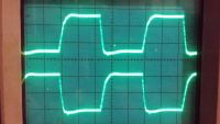
Graham Armitage, Sat Jan 10 2015, 03:39AMThis is the voltage pattern at the two gates of the IGBT. No ringing which is good, but a little worried by the rise time. 2uS/div and 20v/Div on the display. Running UD2.5 driver. This is driving a CM300DY-24H IGBT but I still fee like it should be a little faster. No bus voltage applied. H-Bridge design attached. Interested to hear anyone's feedback on this and if it's acceptable?

Re: Gate Voltage
Kolas, Sat Jan 10 2015, 09:55AM
As far as I can tell, the driving of the gate to the maximum voltage is to insure complete saturation, and the datasheet says that the VGE(th) is 7.5v max. It appears to attain that voltage far faster then your switching frequency. so without any other knowledge then that, I'd be willing to believe that it is acceptable.
Re: Gate Voltage
Kizmo, Sat Jan 10 2015, 12:51PM
Its easily fast enough. General rule of thumb is that you want to switch as slowly as possible. I had CM600 coil which ran at around 3000A and gate rise/fall times were little bit 1µs at 41kHz. No problems.
Kizmo, Sat Jan 10 2015, 12:51PM
Its easily fast enough. General rule of thumb is that you want to switch as slowly as possible. I had CM600 coil which ran at around 3000A and gate rise/fall times were little bit 1µs at 41kHz. No problems.
Re: Gate Voltage
Graham Armitage, Sat Jan 10 2015, 03:27PM
Thanks all - glad to hear this looks ok.
Graham Armitage, Sat Jan 10 2015, 03:27PM
Thanks all - glad to hear this looks ok.
Re: Gate Voltage
Graham Armitage, Sun Jan 11 2015, 03:39PM
Ok, maybe it's been a long night huddled over the coil, but this is not making any sense. Trying to tune for ZVS and getting some plain weird results as shown in the image. I have one probe on one of the gates and the other at the E1/C2 bridge output. The square wave is the gate signal. What is confusing is that the frequencies of the two signals don't match. I can shift the phase with the variable inductor, but the rising and falling edges of both signals should be in sync. Any ideas what's going on here?
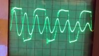
Well, it seems my scope may be the problem. with no grounds connected it's picking up some strange freq. By turning up the bus voltage to around 40v I was able to eliminate that and now see two signals in sync, but slightly out of phase. What is still odd is that the one gate voltage is 1/2 the other one. When I disconnect the GDT the outputs from the UD2.5 are both +-24v. Could this be an IGBT issue?
Another question - when setting ZVS phase, which gate should one probe, or does it matter?
Graham Armitage, Sun Jan 11 2015, 03:39PM
Ok, maybe it's been a long night huddled over the coil, but this is not making any sense. Trying to tune for ZVS and getting some plain weird results as shown in the image. I have one probe on one of the gates and the other at the E1/C2 bridge output. The square wave is the gate signal. What is confusing is that the frequencies of the two signals don't match. I can shift the phase with the variable inductor, but the rising and falling edges of both signals should be in sync. Any ideas what's going on here?

Well, it seems my scope may be the problem. with no grounds connected it's picking up some strange freq. By turning up the bus voltage to around 40v I was able to eliminate that and now see two signals in sync, but slightly out of phase. What is still odd is that the one gate voltage is 1/2 the other one. When I disconnect the GDT the outputs from the UD2.5 are both +-24v. Could this be an IGBT issue?
Another question - when setting ZVS phase, which gate should one probe, or does it matter?
Re: Gate Voltage
Mads Barnkob, Sun Jan 11 2015, 06:59PM
It is the inverter voltage output versus the primary current you have to sync in order to obtain ZCS.
Mads Barnkob, Sun Jan 11 2015, 06:59PM
Graham Armitage wrote ...
Well, it seems my scope may be the problem. with no grounds connected it's picking up some strange freq. By turning up the bus voltage to around 40v I was able to eliminate that and now see two signals in sync, but slightly out of phase. What is still odd is that the one gate voltage is 1/2 the other one. When I disconnect the GDT the outputs from the UD2.5 are both +-24v. Could this be an IGBT issue?
Another question - when setting ZVS phase, which gate should one probe, or does it matter?
It is the inverter voltage output versus the primary current you have to sync in order to obtain ZCS.
Re: Gate Voltage
Graham Armitage, Sun Jan 11 2015, 07:27PM
I understand that we want to switch the transistors when the current is zero, but there is a phase difference between the voltage and the current in the primary circuit correct? So where should those current measurements be taken? I see some people scoping bus voltage and gate voltage. I have been looking for a simple test procedure to figure this out.
Too complicate things, I have a 100MHz analog scope and taking measurements on the primary circuit without ground connections is causing very noisy signals so I am not sure what I am seeing is an accurate representation of what's really happening. Any suggestions on reducing this? I am testing with an isolated DC power supply - 30-40V
Graham Armitage, Sun Jan 11 2015, 07:27PM
Mads Barnkob wrote ...
It is the inverter voltage output versus the primary current you have to sync in order to obtain ZCS.
It is the inverter voltage output versus the primary current you have to sync in order to obtain ZCS.
I understand that we want to switch the transistors when the current is zero, but there is a phase difference between the voltage and the current in the primary circuit correct? So where should those current measurements be taken? I see some people scoping bus voltage and gate voltage.
 I have been looking for a simple test procedure to figure this out.
Too complicate things, I have a 100MHz analog scope and taking measurements on the primary circuit without ground connections is causing very noisy signals so I am not sure what I am seeing is an accurate representation of what's really happening. Any suggestions on reducing this? I am testing with an isolated DC power supply - 30-40V
Re: Gate Voltage
Steve Ward, Sun Jan 11 2015, 07:54PM
If you are on isolated power, you can connect the scope ground clip to the -DC bus as your reference.
Your remark about gate voltages changing sounds like you are just measuring the gate voltage plus the source voltage on the top IGBT, so of course it looks funny. You cannot easily scope a high-side and low-side gate simultaneously, under power.
My suggestion is to look at the switch node (connection between top/bottom IGBT) along with the low-side gate, with the scope clips on the -DC bus as reference (preferably as close to the IGBT terminal as possible). Ideal switching conditions will give minimal ringing on both Vge at turn on, and Vce in both directions. I usually observe the Vce (switch node) vs primary current to tune the phase lead inductance for optimal switching. I find optimal timing to be such that the IGBT begins turning off before the primary current has hit zero current, perhaps some 10-20 degrees ahead of that. Going too far from ZCS will result in large overshoot as you are "hard switching", and so a voltage is produced across the switch inductance proportional to dI/dt. Switching more than Ic-nominal should be avoided.
Its extremely helpful to have a current transformer to scope out as well. Watch out for induced voltages on home-made CTs, keep all external wiring loops to a minimum by using co-ax or twisted pair techniques. A simple wire loop near a high-current RF circuit will experience significant EMF that adds in with your desired signals.
Re: Gate Voltage
Graham Armitage, Sun Jan 11 2015, 08:32PM
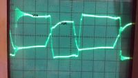
Steve, thank you very much. This is super helpful. First off, I referenced the scope clips to the neg DC bus and that solved the noise problem. As you suggested I connected the one probe to the E1/C2 connection and the other probe to the G2 terminal. The resulting wave form is interesting. The switching on the falling edge looks perfect with minimal ringing on the primary. On the rising edge is where things seem to go wrong. It looks like the gate is turning off way to soon and we get a lot of ringing. As you can see from the first image on this thread the Vge pattern looks great without any bus voltage. What would cause the one side to behave different from the other?

Re: Gate Voltage
Kolas, Mon Jan 12 2015, 03:44PM
I personally cannot fathom why that waveform looks the way it does, but I can be reasonably sure that you DO NOT want to operate it with much power when it's doing that right there. Shoot through is a killer. If i was seeing that, i might look at the length (or difference in) your GDT wiring from igbt to igbt.
Re: Gate Voltage
Graham Armitage, Mon Jan 12 2015, 04:33PM
I agree. That's why I am hesitating on going beyond test phase. What I keep seeing is that the voltage on G1 looks much better. Without the bridge connected both legs of the GDT have perfect wave-form. I am wondering if something is going on with the second IGBT in the bridge. Tonight I might try and switch the two gate connections from the GDT and see if that changes anything. Both gate leads from GDT are 3" long and tightly twisted.
Re: Gate Voltage
Steve Ward, Mon Jan 12 2015, 07:50PM
Is this just a half-bridge drive (not full H-bridge)? If so, its often necessary to "manually" discharge the primary capacitor with a bleeder resistors. My suggestion would be to try a pair of 20K, 10W power resistors placed from the C1 to C2E1 terminal and from the C2E1 to the E2 terminal. This should look like a resistor in parallel with each IGBT and the effect is that the MMC will be charged to 1/2Vbus between firings. This should happen naturally but often doesn't, and should the primary C have significant charge at start up, there can be a "DC" component that messes with the duty cycle of the driver (which is what i think im seeing in your scope shot).
If you look after many more cycles, does the Vce waveform look more symmetrical?
Differences in ringing on rising/falling edge can also be a matter of perspective. Assuming an isolated power source, you can alternately scope the Vce of the top switch by connecting scope ground to the +DC rail and "invert" the scope channel. The result is often that the turn-on looks cleaner across the measured switch, than the turn-off (assuming you switch before the current reverses).
Side note: You cannot easily measure Vge of the top IGBT, however. I should also say that putting scope ground on the switch-node is not a good idea in general when switching significant voltage. Special isolation type scope probes would be useful for measuring signals referenced to switched voltages.
Re: Gate Voltage
Graham Armitage, Mon Jan 12 2015, 08:30PM
This is an H-Bridge. Single brick with two transistors. Your point about the resistors is a great suggestion. I have 2 10W (6k) resistors across the bus capacitor at the IGBT. But that means they are not connected to C1/E2 - that could be significant. I will try fix that tonight. maybe go with 20k as you suggest before I run it at power.
I will check again, but I don't believe the waveform changed after multiple cycles. I can see how measuring Vge on the top gate is problematic. The idea of "referencing" on the +DC and inverting is clever. I will try that as well and see if it looks any different. Will post my findings later tonight. Thanks for all the suggestions

Re: Gate Voltage
Antonio, Mon Jan 12 2015, 11:41PM
Do you have a capacitor in series with the primary winding of the GDT? This may cause asymmetries. Look if the waveform stabilizes after some cycles of the burst. And look carefully at where are the ground connections of the oscilloscope. You can, in principle, ground the oscilloscope at the negative rail (if it is insulated from the mains ground) and look at the outputs of the bridge and at the gates of the lower transistors. Asymmetries would appear also at the primary side of the GDT, where it's safer to observe them with a normal ground.
Re: Gate Voltage
Graham Armitage, Tue Jan 13 2015, 02:43AM
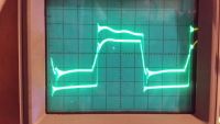
Making progress!! Tried checking the G1 waveform by inverting the signal and got the same weird behavior. Next I tried adding 6k resistors across the CE of the IGBTs - still the same. What was strange was as i changed the pulse width or frequency the phase would shift and it was difficult to get a proper measurement. So I tried adding a 10uF tantalum cap in series with the one output to the GDT - voila !! Immediately my GDT started singing like a canary (what I am used to hearing) and the bus current draw increased. Seemed to be getting much higher primary currents too. image below shows the Vge (smaller wave) and the bridge output with minimal ringing. There was quite a bit of ringing but as I tuned the inductor it disappeared.
I have not heard or read of the UD2.5 needing the 10uF cap, but I had it on a previous driver circuit. The UD2.5 has 2 1uF caps - would it make sense to remove those and replace it with the 10uF? This is my first UD2.5 build.

Re: Gate Voltage
Graham Armitage, Wed Jan 14 2015, 12:34AM
Well I figured out what was causing the problem on the falling edge on the gate voltage... initially thought it was adding a capacitor to the gate drive output, but it didn't matter what value I used. Then I realized I was switching the wires when adding the capacitor. So I removed the cap and switched the wires - everything works. Now I have NO idea why that would be, but I am leaving it as is for now. Maybe someone smarter than me has some clue.
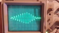
When playing with the tuning I did see some other strange behavior. Increasing inductance would reduce ringing at the beginning of the oscillations but increases it toward the end. This 12s video shows what I mean. Is this a symptom of something else? Could it be something the scope is picking up and not really an issue. I have low confidence in this scope right now, but have nothing else to set this ZCS.
The current on the primary seems to be behaving nicely
Graham Armitage, Wed Jan 14 2015, 12:34AM
Well I figured out what was causing the problem on the falling edge on the gate voltage... initially thought it was adding a capacitor to the gate drive output, but it didn't matter what value I used. Then I realized I was switching the wires when adding the capacitor. So I removed the cap and switched the wires - everything works. Now I have NO idea why that would be, but I am leaving it as is for now. Maybe someone smarter than me has some clue.
When playing with the tuning I did see some other strange behavior. Increasing inductance would reduce ringing at the beginning of the oscillations but increases it toward the end. This 12s video
 shows what I mean. Is this a symptom of something else? Could it be something the scope is picking up and not really an issue. I have low confidence in this scope right now, but have nothing else to set this ZCS.
The current on the primary seems to be behaving nicely


Re: Gate Voltage
loneoceans, Wed Jan 14 2015, 12:42AM
That's expected behavior. My page on the UD2.7 describes a general tuning procedure which will be useful for this. Your scope is fine by the way - I actually prefer analog scopes for catching spikes like these.
loneoceans, Wed Jan 14 2015, 12:42AM
That's expected behavior. My page on the UD2.7 describes a general tuning procedure which will be useful for this. Your scope is fine by the way - I actually prefer analog scopes for catching spikes like these.
Re: Gate Voltage
Graham Armitage, Wed Jan 14 2015, 01:17AM
I totally missed that when looking at your site. This makes me feel much better - I see exactly what you show. Makes total sense to reduce the ringing at the end of the oscillations when current is highest. Glad my scope is not lying but I still think I need a nice new shiny digital storage scope
Thanks again to everyone for help on this. Hopefully post some photos of it in operation soon.
Graham Armitage, Wed Jan 14 2015, 01:17AM
I totally missed that when looking at your site. This makes me feel much better - I see exactly what you show. Makes total sense to reduce the ringing at the end of the oscillations when current is highest. Glad my scope is not lying but I still think I need a nice new shiny digital storage scope

Thanks again to everyone for help on this. Hopefully post some photos of it in operation soon.
Re: Gate Voltage
Graham Armitage, Wed Jan 14 2015, 02:30AM
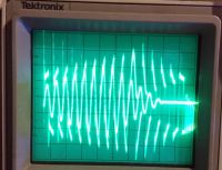
One last observation for the evening. The tuning seems to be fine and ringing eliminated at the end of the cycle. This is the bridge output and primary current with the bus voltage at around 100v. I would have expected the bridge output waveform to be a little more square and less spikey?

Print this page