
Simple and robust flyback voltage converter
Yandersen, Sun Aug 04 2013, 07:37PMThe goals of the following design is:
1) Minimum part count
2) Maximum efficiency over all operating voltage range (including ~0V range) to eliminate heatsinking requirements
3) No-cap-in-load detection and circuit protection
4) Automatic shut-off when cap repolarization detected (major recuperational gauss design and induction coilgun issue)
Here is the first version of the proposed circuit:

Re: Simple and robust flyback voltage converter
Yandersen, Sun Aug 04 2013, 08:29PM
The following cycling operation is assumed:
1) Initially there is no current flowing through Rctrl, so In pin of left driver is 0 and Out pin goes high, opening the K1 MOSFET.
2) Current building up in the transformer while Cf cap is discharged through Rf.
3) After some time Cf discharged down to the LOW threshold level of the Enable pin of the left driver, forcing it's Out to go LOW, switching off the K1 in result.
4) When MOSFET closes, voltage over the primary and secondary of the transformer inverts and current starts to flow through Dhv to the output cap. It also runs through Rctrl chain, so voltage on the In pin of the left driver is over HIGH threshold which forces it's output to be LOW.
5) While K1 is closed, Cf is charged up to the voltage level, clamped by DZ1. This level is assumed to be just a little over the HIGH threshold of the Enable pin of the left driver (3-4V for most drivers). Cf reaches it's up bound very fast, so driver gets enabled pretty soon. But it can't go HIGH until it's In will fall down to LOW threshold level. And this will not happen until the current in the secondary will deplete to the minimum level determined by Rctrl chain resistance and LOW threshold level of the In pin of the left driver. As a result, K1 is not getting open again until transformer is ready for another portion of the input current. This way short-circuiting of the output becomes a normal operation mode for this voltage converter.
As a result, the time transformer is sucking current from the supply is always constant and independent from the input or output voltage (input voltage is assumed to be const). But the second part of the cycle, when trans drains to the load, has a variable timing which controlled by the output current - first cycle is not started again until the current depletes to the certain level. This current-controlled timing lets achieve almost the same efficiency level over all output voltage range. Average output current is close to const resulting in a constant speed of cap voltage rise speed over the whole range of voltage.
The right driver and K2 are the major protection elements. During a shot of an induction coilgun or recuperational gauss gun (those use non-polar caps) caps' voltage is inverted. When it happens, current through Rctrl chain increases greatly as cap starts to discharge through the secondary of the trans and output diode. If load is not disconnected fast, the secondary and Dhv will burn. The overcurrent case is sensed by Rctrl chain. If voltage on Ra rises to the HIGH threshold of the right driver, it switches it's Out to LOW, forcing K2 to close disconnecting the Cload. Together with K2 the Enable pin of the right driver goes LOW, latching the driver in a LOW output state even when it's In goes LOW again as a result of current stop running through Rctrl. The system is halted up untill Cpause is charged back to the HIGH threshold of Enable pin through built-in pullup resistor (all MOSFET drivers with Enable have those). When it happens, right driver opens again. If Cload is still inverted, latch happens again. System will try to reboot until the Cload will return to the proper polarity.
If Cload is not connected at all, then on the second cycle voltage of the K1' drain will jump high to the level clamped by DZ2+DZ3+0.6V of D2. If it will happen, the current through Rctrl will be very high and right driver will sense it the same way as inverted polarity of the Cload, halting the converter the same way.
Output voltage control circuit I used to is a chain of zener diodes and optocoupler.
Re: Simple and robust flyback voltage converter
Yandersen, Sun Aug 04 2013, 08:36PM
Will appreciate any feedback, tests or modelling in Spice or wherever else. Free to use, duplicate, repost, upgrade. :)
Yandersen, Sun Aug 04 2013, 08:36PM
Will appreciate any feedback, tests or modelling in Spice or wherever else. Free to use, duplicate, repost, upgrade. :)
Re: Simple and robust flyback voltage converter
Yandersen, Fri Aug 16 2013, 05:00AM
New version. Still not tested, just based on previous practical experience, calculations and datasheets:

Notes:
Time constant of the part of the cycle when transformer sucks the current from supply is determined by R1 and Cf. It is approximately equal to 2*R*C seconds (if Cf is 330pF then trans will charge for ~20us). The second part of cycle, when Q1 is off and current flows through secondary into load lasts until the output current falls to the certain level. This relaxation time depends on the output voltage at the moment - the higher it is, the faster the transformer empties it's stored energy. The new current build-up cycle starts when voltage at In2 falls below LOW input level which is around 1.3V for the IC used in schematic. F.e. if you want the new cycle to start when output current falls down to 100mA, then use R2+R3=13Ohm. Assume you decided the protection current to be 10A. If so, then R3 is 0.15Ohm and R2 is 12.85Ohm.
The DZ3 and DZ4 zeners are for protection only. Those should not pay a part in normal operation. Only in error conditions the current flows through them.
The DZ1 activates the protection sequence in case output cap is not connected. It's zener voltage should be picked in accordance to the Q1 maximum drain voltage:
Vz(DZ1) = Vd(Q1)-Vz(DZ3)-Vz(DZ4)-Vf(D1) Volts.
If maximum drain-source voltage of Q1 is 50V, then using 43V as DZ1 should do the work.
The repetitive reverse voltage rating of output rectifier, D2, should be two times higher than output voltage the charger is designed for. For 400V cap charger the 800V diode should be used. Pay attention to the surge current rating - diode must be able to sustain without damage the overcurrenting (10A in the example above) for 10us at least.
D4 is the diode with low-leakage current rating and reverse voltage rating at least equal to the output voltage the charger is designed for.
DZv is a chain of zener diodes. The sum of their's zener voltages determine the shut-down output voltage level. F.e. for 400V charger two 200V zeners may be used. Use ones with minimum power rating to minimize the leakage current. One TVS instead of chain of zeners will not work due to low precision and high leakage.
Q2 is the main protection element of the charger. If any error condition determined (no load, over-currenting, output voltage level reached) it is closed by driver1 effectively disconnecting the charger from the load. The drain-source voltage of Q1 must be at least equal to the output voltage the charger is designed for (double rating will be better). Q1 must be able to sustain surge current during overcurrenting without damage (10A in the example above). Choose the one with low on-resistance rating as most of the time this MOSFET stays in ON state and it is not switched frequently.
D3 and D5 are low-voltage (20V) pulse diodes (~2A at surge) with preferably low leakage current (<1uA below 6V).
C3 is a filter cap and must have lowest ESR possible (think about ceramic caps) and be connected as close as possible to the IC' Vcc and Gnd pins.
C1 is an electrolithic cap with high ripple-current rating (at least equal to the peak current in the primary at the end of current-suck cycle). It's "+" must be as close as possible to the trans' primary and "-" is close to the source-pin of Q1 to minimize the parasitic inductance and resistance in a Q1-C1-Tprim loop.
Re: Simple and robust flyback voltage converter
DerAlbi, Fri Aug 16 2013, 10:23AM
blablabla i dont like the design, the schematic is cryptic, and.. well hiere was once a lot of more text. i deleted it
the design could work, but there is no benefit over ordering a free sample of the LT3750 and build the stuff the easy way. should be much cheaper too.
edit2: my edit and your following text came up at the same time. f....
edit3: thanks for your added description. helps a lot.
Re: Simple and robust flyback voltage converter
Yandersen, Fri Aug 16 2013, 05:01PM
blablabla - can't delete outdated reply by myself.
Yandersen, Fri Aug 16 2013, 05:01PM
blablabla - can't delete outdated reply by myself.
Re: Simple and robust flyback voltage converter
Yandersen, Mon Aug 19 2013, 06:35PM
That is what I'm planning to try to build after all:

Output current-controlled flyback voltage converter for capacitors charging. Actively-protected from the following error conditions:
1) No capacitor in load connected;
2) Load capacitor repolarized;
*Short circuit at output is considered to be normal operating condition.
Preset numbers:
[IPrimPeak] Amperes is a peak value of current flowing into primary winding of the transformer during the feed cycle when current is building up;
[ISecPeak] and [ISecMin] Amperes is a maximum and minimum values of the current, respectively, flowing from secondary winding of the transformer into load during the output cycle;
[IProtect] Amperes is a current flowing through secondary during the error conditions for a short period of time (~10us);
[VOut] Volts is an output voltage the converter is designed for;
Parts:
R2 and R3 are current-controlling resistors with 3:1 resistance ratio (NOT wire-wound - metal-oxide or carbon, with minimum parasitic inductance). Their sum resistance (R2+R3) is determined by the [ISecMin] value:
R2+R3 = ( 1.3 / [ISecMin] ) Ohm;
[IProtect] can be calculated then as (1.3 / R3) A or simply 4*[ISecMin].
Keep in mind that [ISecPeak] must be less than [IProtect] and is recommended to be {2...3}*[ISecMin].
D1: 20V, [IPrimPeak] A surge current rated;
D2: 2*[VOut] V, fast switching diode, [IProtect] A surge current rated, [ISecPeak] A repetitive pulse current;
D3: 20V, low-leakage, low forward voltage drop diode, [IProtect] A surge current rated;
D4: [VOut] V, general purpose diode with low leakage current;
D5: 20V, low-leakage, 3A surge current rated;
D6: 20V, [IProtect] A surge current rated, preferably low parasitic capacitance at Vr=12V;
Q1: minimum 40V drain-source voltage;
DZ1: 12V less than Vds of Q1 (DZ1=28V for 40V MOSFET), [IPrimPeak] A surge current rated;
Q2: [VOut] V, [IProtect] A surge current rated MOSFET with preferably low Rds rather than low Qg;
DZv is a chain of low-power zener diodes with low leakage current, connected in series for performing a voltage-control function; total zener voltage of the chain should be a couple volts lower than [VOut] V.
Cf is a cap controlling the duration of the feed cycle (when Q1 is open and transformer sucks current from supply through the primary winding). This time constant is roughly equal to (1.5*Cf*R1) seconds. To choose Cf precisely, put a resistor in place of primary transformer winding and using the oscilloscope check the time the resistor holds 12V voltage drop on it. To double this value, use double capacity cap and so on. Keep in mind that feed cycle starts with transformer not completely deenergized as switching performed at [ISecMin] A, not at 0 A (so derate saturation time).
Notes:
The effective turns ratio of the transfomer is recommended to be 12:(0.5*[VOut]). This way the average duration of the output cycle over the whole output voltage range will be equal to the constant duration of the feed cycle.
Yandersen, Mon Aug 19 2013, 06:35PM
That is what I'm planning to try to build after all:
Output current-controlled flyback voltage converter for capacitors charging. Actively-protected from the following error conditions:
1) No capacitor in load connected;
2) Load capacitor repolarized;
*Short circuit at output is considered to be normal operating condition.
Preset numbers:
[IPrimPeak] Amperes is a peak value of current flowing into primary winding of the transformer during the feed cycle when current is building up;
[ISecPeak] and [ISecMin] Amperes is a maximum and minimum values of the current, respectively, flowing from secondary winding of the transformer into load during the output cycle;
[IProtect] Amperes is a current flowing through secondary during the error conditions for a short period of time (~10us);
[VOut] Volts is an output voltage the converter is designed for;
Parts:
R2 and R3 are current-controlling resistors with 3:1 resistance ratio (NOT wire-wound - metal-oxide or carbon, with minimum parasitic inductance). Their sum resistance (R2+R3) is determined by the [ISecMin] value:
R2+R3 = ( 1.3 / [ISecMin] ) Ohm;
[IProtect] can be calculated then as (1.3 / R3) A or simply 4*[ISecMin].
Keep in mind that [ISecPeak] must be less than [IProtect] and is recommended to be {2...3}*[ISecMin].
D1: 20V, [IPrimPeak] A surge current rated;
D2: 2*[VOut] V, fast switching diode, [IProtect] A surge current rated, [ISecPeak] A repetitive pulse current;
D3: 20V, low-leakage, low forward voltage drop diode, [IProtect] A surge current rated;
D4: [VOut] V, general purpose diode with low leakage current;
D5: 20V, low-leakage, 3A surge current rated;
D6: 20V, [IProtect] A surge current rated, preferably low parasitic capacitance at Vr=12V;
Q1: minimum 40V drain-source voltage;
DZ1: 12V less than Vds of Q1 (DZ1=28V for 40V MOSFET), [IPrimPeak] A surge current rated;
Q2: [VOut] V, [IProtect] A surge current rated MOSFET with preferably low Rds rather than low Qg;
DZv is a chain of low-power zener diodes with low leakage current, connected in series for performing a voltage-control function; total zener voltage of the chain should be a couple volts lower than [VOut] V.
Cf is a cap controlling the duration of the feed cycle (when Q1 is open and transformer sucks current from supply through the primary winding). This time constant is roughly equal to (1.5*Cf*R1) seconds. To choose Cf precisely, put a resistor in place of primary transformer winding and using the oscilloscope check the time the resistor holds 12V voltage drop on it. To double this value, use double capacity cap and so on. Keep in mind that feed cycle starts with transformer not completely deenergized as switching performed at [ISecMin] A, not at 0 A (so derate saturation time).
Notes:
The effective turns ratio of the transfomer is recommended to be 12:(0.5*[VOut]). This way the average duration of the output cycle over the whole output voltage range will be equal to the constant duration of the feed cycle.
Re: Simple and robust flyback voltage converter
Steve Conner, Thu Aug 22 2013, 09:31AM
Why don't you just use one of the UC3842 family. Nice simple current-mode controller. Jan Martis made a great flyback driver with it.
Steve Conner, Thu Aug 22 2013, 09:31AM
Why don't you just use one of the UC3842 family. Nice simple current-mode controller. Jan Martis made a great flyback driver with it.
Re: Simple and robust flyback voltage converter
Yandersen, Thu Aug 22 2013, 11:03AM
Lower output current, predetermined functionality. I mean, designing the charger with UC3842 comes to designing the charger based on that IC. But I needed to made a charger with some unusual functionality, so I made a circuit based on simple elements, and MOSFET driver I used is an industry-standard device with simple functionality, MCP14E9 is 3A peak, MCP14E3 is 4A peak, MCP14E6 is 2A, and there are plenty of other drivers all of the same kind.
If all functionality my charger has can be achieved with smg like UC3842 with lower external elements count - well, this would be even better. But I can not design a multifunctional_IC-based charger without having that IC physically tested first (I had an unexpected glithes even with 556 timers) as datasheets are always missing smg and for multifunction IC those pages are always undescriptive. What are the propagation delays, for example? How can I implement a protection logic with undeterminable reaction time on hazardous conditions? MOSFET drivers are simple to implement in a new design and those are all fully-specified and fast.
Anyway, I have parts coming soon, will see how my device will work.
Re: Simple and robust flyback voltage converter
Erlend^SE, Thu Aug 22 2013, 04:15PM
UC3842:
No cap voltage: limit voltage on comp-pin.
No cap protection: use some smaller capacitor on a seperate winding to detect too big peaks and drive the comp-pin low (disables the IC)
Polarity reversal: There is no switch in the route (coil & diode only), but limiting the comp-voltage should limit the PWM to safe values. or drive comp low (1 cycle or less?) Given it's not isolated, a direct sense should be doable.
The chip got built-in FET-driver, and can in some cases regulate it's own voltage from external supply.
Re: Simple and robust flyback voltage converter
Yandersen, Fri Aug 23 2013, 03:57AM
The Q2 is essential. The reversed voltage on a non-polar cap may stay infinitely. Due to that problem I have already burned a dozen of parts forgetting to unload the repolarized cap. Right now I'm considering the option of coupling two chargers to use caps in both polarities, reversing it each next shot, this way I can use 1 cap per each stage eliminating the need of coupled stages which reuse leftover energies.
Well, if you want to present a schematic based on other IC - go on moderning the circuit, maybe it will be better then mine. But I will first try to build my idea as I already ordered the parts.
Re: Simple and robust flyback voltage converter
Yandersen, Tue Aug 27 2013, 09:08PM
Tested some parts of the design in practice. Guys, need help to find IC with some built-in functions.
The ideal IC must have the following functions:
1) 2 FET drivers;
2) at least 1 voltage comparator able to operate near the ground level with <1us response time (including 0-Vcc output swing);
3) undervoltage protection - outputs of the FET drivers must not go high if supply voltage is below 6-10V.
Any suggestions?
Re: Simple and robust flyback voltage converter
Yandersen, Mon Sept 16 2013, 09:51PM
After the practical tests some updates are made to the schematic:

Two chargers built by the schematic above are planned to be connected antiparallel to charge non-polar caps both directions:

Yandersen, Mon Sept 16 2013, 09:51PM
After the practical tests some updates are made to the schematic:

Two chargers built by the schematic above are planned to be connected antiparallel to charge non-polar caps both directions:

Re: Simple and robust flyback voltage converter
Yandersen, Wed Sept 18 2013, 12:21AM
Ordered two EPCOS' p-cores to make a couple of transformers. Here is what I got:

The first one who will guess right what is wrong on that picture, will have a candy! :)
Yandersen, Wed Sept 18 2013, 12:21AM
Ordered two EPCOS' p-cores to make a couple of transformers. Here is what I got:

The first one who will guess right what is wrong on that picture, will have a candy! :)
Re: Simple and robust flyback voltage converter
Yandersen, Sat Oct 19 2013, 07:15AM
Finally got rid of all bugs in the concept. The final schematic is the following:

Yandersen, Sat Oct 19 2013, 07:15AM
Finally got rid of all bugs in the concept. The final schematic is the following:

Re: Simple and robust flyback voltage converter
Yandersen, Sat Oct 19 2013, 07:21AM
My pcb board (7cm x 5cm):

This is a 780V converter version of the schematic above.
It gave me 126W output at 751V with resistive load (light bulbs) consuming 138.6W from the supply (90.9% efficiency). All the features are confirmed to be working fine, no power-up and shut-down glitches.
Cap 60uF charged to 760V in 0.15 seconds. It gives average power for capacitive loads 115W.
Hm, 2 and a half month designing the charger...
Re: Simple and robust flyback voltage converter
Thomas W, Sat Oct 19 2013, 10:49AM
Very nice project here!
how did you manage to solder on that cheap chinese matrix board? i have a load of those... couldnt use them as ever time i tried to solder onto them, the copper track pads keep coming off :c
Thomas W, Sat Oct 19 2013, 10:49AM
Very nice project here!
how did you manage to solder on that cheap chinese matrix board? i have a load of those... couldnt use them as ever time i tried to solder onto them, the copper track pads keep coming off :c
Re: Simple and robust flyback voltage converter
Yandersen, Sun Oct 20 2013, 04:55PM
Yeah, that is true - desoldering and replacing parts leaves empty spaces underneath. That is why I used a new matrix board for every other version (good I have hundred of those little boards - still didn't ran out).
To make tracks I just bend legs of the resistors under the board forming tracks. At some point it is even better then normal pcb approach as lines are formed with relatively thick copper. :)
Re: Simple and robust flyback voltage converter
Steve Conner, Mon Oct 21 2013, 09:34AM
Well done, good efficiency! :) What is the function of Q2 in your circuit?
Steve Conner, Mon Oct 21 2013, 09:34AM
Well done, good efficiency! :) What is the function of Q2 in your circuit?
Re: Simple and robust flyback voltage converter
Yandersen, Mon Oct 21 2013, 02:35PM
This is a protection from cap repolarization. See, as I am using non-polar caps without reverse diode, when I shot, cap discharges onto coil, then coil charges cap with hundred of Amps in reverse polarity. Standard charger, if not disconnected, will blow. My charger actively determines cap repolarization by the increased output current, and shuts down, closing the Q2. Every 30-40ms it opens Q2 for couple us to check if cap is still repolaried. It draws tiny amount of energy from cap. The Q2 closes permanently when supply voltage drops below 10V or so as when supply disconnected, so it is safe to shut down or turn on the gun with caps in reverse polarity.
Making further testings I discovered that no-cap-in-load protection (when the output wire broken and charger outputs into air) doesn't work that well. Albi recommended me to have cap on charger side, like a minimum load, but it is not that easy to implement in my design due to existence of Q2. Working on it now...
The efficiency in my setup may be couple percent higher when I rewind the trans in more optimal way. Measuring current output instead of input current (which is more common, as I see) is much more efficient and losses on that are negligible. In my setup, ~2V are taken from output voltage for current measuring purposes, which contributes to <0.3% efficiency drop on 780V output. All other losses (output diode, MOSFET, transformer, driver) are the same unavoidable as in any other flyback setup. Using the Silicon Carbide Schottky diode (no reverse recovery current) on output allowed me to implement continuous current mode to lower resistance losses by 25% due to smaller peak currents for the same output power comparing to discontinuous mode.
Re: Simple and robust flyback voltage converter
DerAlbi, Wed Oct 23 2013, 09:51AM
Man, did i just hear my name
^_^
Now everyone knows we're without a life hanging around skype each day developing the biggest doomsday machine ever. Maybe i should spoiler my charger too.
Btw if yan and i stop posting, maybe the CIA assassinated us....
...or if just yan stops posting, hes maybe assassinated for trolling the forum. -.-
Re: Simple and robust flyback voltage converter
Yandersen, Wed Oct 23 2013, 10:25AM
No, guys, Albi is a very intelligent guy, he is just tired a little bit of building his doomsday machine from dawn till dusk.
Yandersen, Wed Oct 23 2013, 10:25AM
No, guys, Albi is a very intelligent guy, he is just tired a little bit of building his doomsday machine from dawn till dusk.
Re: Simple and robust flyback voltage converter
DerAlbi, Fri Oct 25 2013, 10:23AM
Yan allowed me to hijack his thread and maybe show an other - more powerfull approach to charging caps . It somehow fits in the thread though, because the design in its basic principle is also verry simple. Of course the whole system is more complex, but the difference to Yans charger, my circuit has clear functional blocks, instead of one big blob that spits out voltage. So overall complexity is greatly reduced.
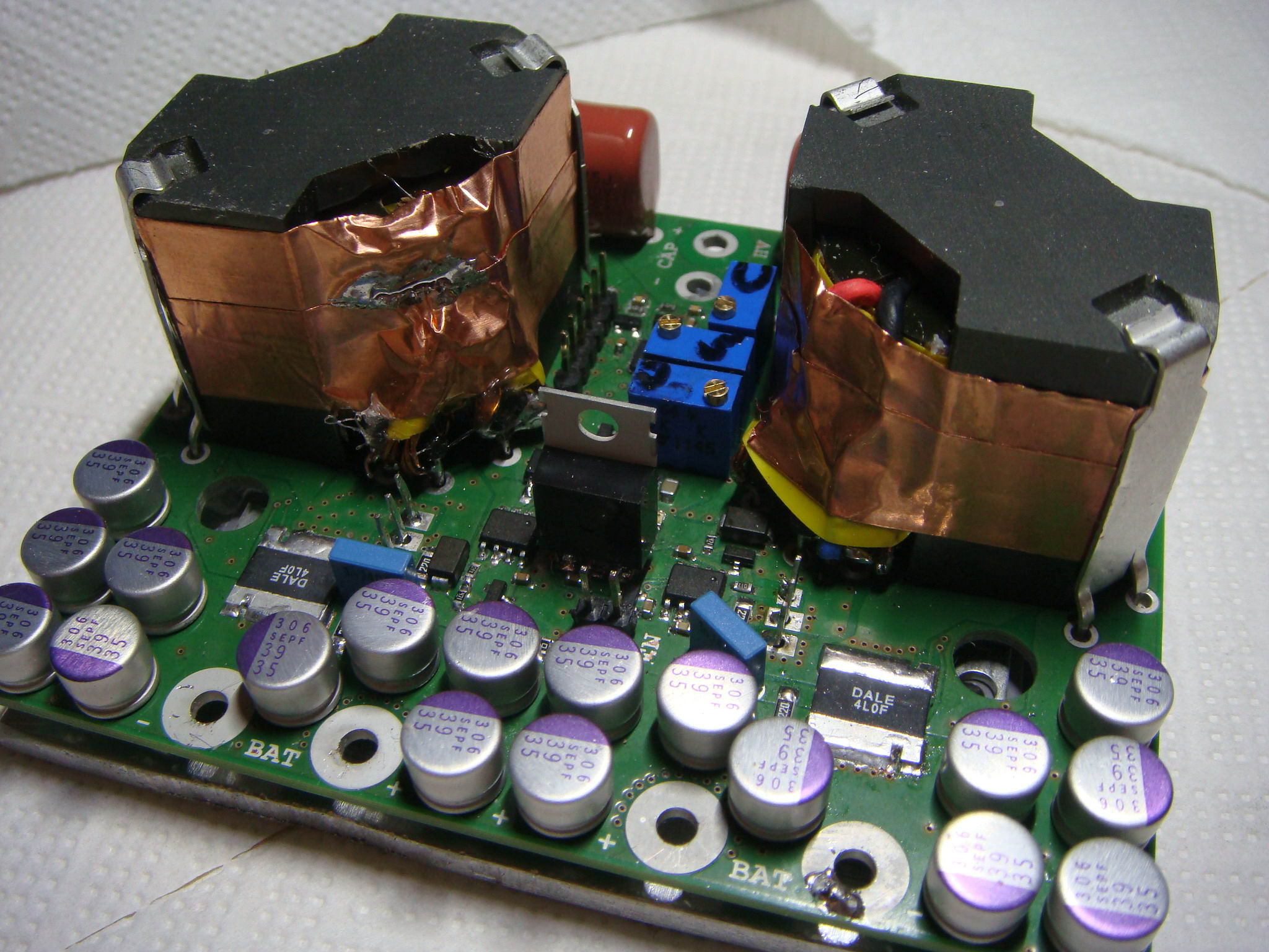
I have designed a two phase discontiousmode Flyback with around >420W output power. Its a four-layer PCB due to the high current paths, and has two self wound 1:8 transformers. One phase consists of one transformer and its Mosfet and a current measuring 4mOhm Shunt. Its voltage is amplified and fed into a comparator, that creates some digital signals representing the state of the transformer. The digital part is compressed into one tiniy CPLD which implements all logic and generates the mosfet gate signals. When the output voltage (220-360V) is reached, the converter automatically deceases its peak-current to achieve better efficiency while holding the charge on the caps. Also under continous load like lightbulbs the current reduces to the minimum needed to sustain the output voltage.
The design is input-power limited to around 30A and is designed to operate from 6s LiFePO4 Batteries. (~19V; less uner load).
Efficiency is around 91% in simulations. Real measurements shows somewhat around 87% which is fine with the simulation. Discontinous mode sucks for the ferrite core - so its ok, expected, and given the achieved output power its a good tradeoff. The heat sink is one solid 4mm thick aluminium plate. Its designed to have heat capacitance only, however it successfully ran the device with 420W output power for around 15min without any symptom of overheating.
The thing ran on first go, since it was verry well simulated before (and having a solid layout - FTW).
Here is some wank stuff:
]flyback.zip (more photos, including current waveform over the shunts + load test)[/file]
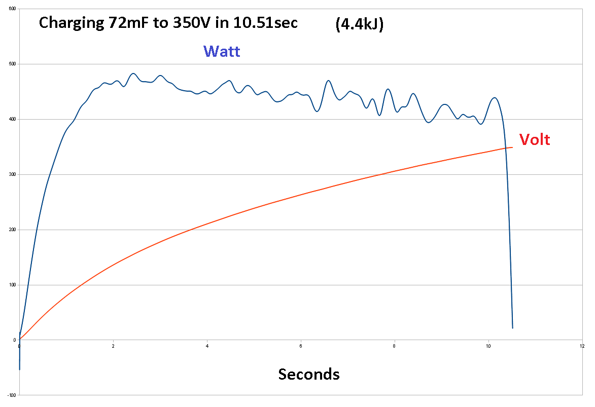
Measured putput power while charging a big capacitive load:
One sweet shot:
If someone feels that i should give away the schematics, please ask. but please keep in mind thats this is Yans thread and you clicked on this topic to discuss HIS design
DerAlbi, Fri Oct 25 2013, 10:23AM
Yan allowed me to hijack his thread and maybe show an other - more powerfull approach to charging caps
. It somehow fits in the thread though, because the design in its basic principle is also verry simple. Of course the whole system is more complex, but the difference to Yans charger, my circuit has clear functional blocks, instead of one big blob that spits out voltage. So overall complexity is greatly reduced.I have designed a two phase discontiousmode Flyback with around >420W output power. Its a four-layer PCB due to the high current paths, and has two self wound 1:8 transformers. One phase consists of one transformer and its Mosfet and a current measuring 4mOhm Shunt. Its voltage is amplified and fed into a comparator, that creates some digital signals representing the state of the transformer. The digital part is compressed into one tiniy CPLD which implements all logic and generates the mosfet gate signals. When the output voltage (220-360V) is reached, the converter automatically deceases its peak-current to achieve better efficiency while holding the charge on the caps. Also under continous load like lightbulbs the current reduces to the minimum needed to sustain the output voltage.
The design is input-power limited to around 30A and is designed to operate from 6s LiFePO4 Batteries. (~19V; less uner load).
Efficiency is around 91% in simulations. Real measurements shows somewhat around 87% which is fine with the simulation. Discontinous mode sucks for the ferrite core - so its ok, expected, and given the achieved output power its a good tradeoff. The heat sink is one solid 4mm thick aluminium plate. Its designed to have heat capacitance only, however it successfully ran the device with 420W output power for around 15min without any symptom of overheating.
The thing ran on first go, since it was verry well simulated before (and having a solid layout - FTW).
Here is some wank stuff:
]flyback.zip (more photos, including current waveform over the shunts + load test)[/file]
Measured putput power while charging a big capacitive load:
One sweet shot:
If someone feels that i should give away the schematics, please ask. but please keep in mind thats this is Yans thread and you clicked on this topic to discuss HIS design
Re: Simple and robust flyback voltage converter
Yandersen, Thu Dec 12 2013, 11:47PM
As a simple version of a flyback converter, here is my simplified schematic:

Design is critical to the transformer quality - high coupling is a requirement. k=99... is good enough. It is achieved by winding transformer like "secondary1-primary-secondary2" (separating secondary by two parts - under and over primary winding). Otherwise the Q1 will burn out all stray inductance' energy in avalanche mode and quickly overheat. 100W of output power is not a problem, radiator on Q1 is required for such power, though. D1 is recommended to be a schottky diode (SiC are awesome) as converter works in continuous mode.
The output current is measured by a voltage drop on R1. When it falls below 1.2V, the new charging cycle starts (Q1 opens). The duration of the charging period is determined by R6 and limited by R7 (in fact, single resistor can be used instead both of those). The minimum duration of discharge cycle is limited by R4.
It is also recommended to put a diode in antiparallel to the output cap C1 in case the output is short-circuited or connected directly to the inductive load (to prevent repolarisation of C1 - it will blow the converter).
And mention that HV- and Gnd are not the same pins, so Gnd can not be used as common ground for HV circuits (conventionally it is, but not here).
Yandersen, Thu Dec 12 2013, 11:47PM
As a simple version of a flyback converter, here is my simplified schematic:
Design is critical to the transformer quality - high coupling is a requirement. k=99... is good enough. It is achieved by winding transformer like "secondary1-primary-secondary2" (separating secondary by two parts - under and over primary winding). Otherwise the Q1 will burn out all stray inductance' energy in avalanche mode and quickly overheat. 100W of output power is not a problem, radiator on Q1 is required for such power, though. D1 is recommended to be a schottky diode (SiC are awesome) as converter works in continuous mode.
The output current is measured by a voltage drop on R1. When it falls below 1.2V, the new charging cycle starts (Q1 opens). The duration of the charging period is determined by R6 and limited by R7 (in fact, single resistor can be used instead both of those). The minimum duration of discharge cycle is limited by R4.
It is also recommended to put a diode in antiparallel to the output cap C1 in case the output is short-circuited or connected directly to the inductive load (to prevent repolarisation of C1 - it will blow the converter).
And mention that HV- and Gnd are not the same pins, so Gnd can not be used as common ground for HV circuits (conventionally it is, but not here).
Print this page