
Low power 433 MHz BPSK data transmission system
WaveRider, Mon May 29 2006, 01:44PMIt's been a while since I have done a radio project. So, I thought I would experiment with data transmission using BPSK (Binary Phase Shift Keying) on the 433 MHz European ISM band.
What's so special about BPSK?
Most commercial systems seem to use frequency shift keying (FSK) or some form of on-off keying (OOK). I wanted to explore the possibilities of constructing a simple system for binary phase shift keying (BPSK). Binary phase shift keying is a form of modulation that is very "power efficient." This means that to achieve a certain bit error rate, the required signal to noise ratio is lower than that required by, e.g., frequency shift keying or on-off keying. BPSK (or QPSK) is often the modulation mode of choice for deep space probes where power consumption must be minimised and signal path losses are enormous. See graphic (taken from
 ) for comparison of error rates....
Why 433.92 MHz?
Besides sitting in the middle of the 433MHz European ISM (industrial, scientific and medical) band, it is also in the amateur 70cm band, so parts were easy to get and it can be modified to operate under amateur radio rules. For those in the US, I think this band also falls under Part 15 of FCC regulations for low-power communications devices. Also, the local oscillators use of-the-shelf SAW resonators instead of a PLL synthesizer. This simplifies the design greatly (at the expense of having to operate on a fixed frequency).
What will the transmitter power be?
Operating below 10mW in this band is permitted without a license. I plan to limit the emissions to somewhat less than this. Many garage door openers and automotive key fobs seem to operate in this band (altho' at much below this power level). Hopefully this won't mean intolerable interference in my experiments!
First step: The receiver design
Since the receiver design is more challenging than the transmitter, I started off there. Here is a block diagram of my proposed receiver.

I am basing the system around the Philips SA639 RF/IF subsystem chip, which is really designed for FSK systems, using a 10.7MHz IF. I managed to find a 500kHz bandwidth ceramic IF filter which should allow upwards of 384kbit/sec communications. BPSK demodulation is not as easy as FSK. Basically, we need to add a carrier regeneration system (a PLL) for demodulating the BPSK signal coherently. I do this with a simple "squaring loop" which doubles the IF carrier frequency. A NE564 PLL/VCO system is the heart of this.
The system
The received signal enters the system (as you would expect
 ) at the antenna input. A low noise amplifier, based on the BFR540 NPN transistor amplifies the antenna signal. I was a bit torn about whether to put the microstrip-based band/image-reject filter before the low noise amplifier. If I put the filter before the amplifier, the filter insertion loss will kill the noise figure of the system. However, putting the filter after the amplifier increases the chances of amplifier overload by strong out-of-band signals. I opted for putting the filter after the amplifier. I will rely on the antenna system to reduce out-of-band signals. Plus, the BFR540 amplifier as I have designed it should be able to withstand -20dBm on the input terminals without saturating.
The next stage is the downconverting mixer. I found a SAW resonator for 423.22MHz which is exactly 10.7MHz away from 433.92MHz. Hence, the local oscillator (based on a BFR92 transistor) fed to the mixer (part of the SA639 chip) downconverts perfectly to 10.7MHz. The ceramic IF filter passes a sharply defined 500kHz channel to the
first IF amp and limiter.
At this point, we split off the signal to the second mixer as well as a push-push active frequency doubler. The output of the doubler is passed through a 21.4MHz (second harmonic) bandpass filter (with a band-stop notch at 10.7MHz) to the PLL carrier regeneration circuit. The 21.4MHz signal is divided by 2 using a flip-flop. After a phase correction and level adjusting circuit, the regenerated carrier is fed to the final mixer, where it is mixed with the original amplitude limited IF signal. The output will be the original BPSK digital data signal (a 250kHz low-pass filter on the output remives any residual RF). A schmitt trigger squares up the output and produces a TTL compatible signal.
I am hoping for a BER at 384kbit/sec of under 10e-6 with -106dBm input at the antenna terminals (in the absence of other interfering transmitters).
Notes
I am at the stage of making the printed circuit board. I can make the schematics available, if people are interested in replicating this work. I will continue to post modifications, measurements and simulation results as I get them.
My main motivation was to experiment with digital transmission of sound and image data for a remote telemetry and surveillance system. I noticed that many commercial systems tend to use FSK, because of its simplicity of implementation. However, for a given power level and a bit of added system complexity, it should be possible achieve improved reception over longer distances using BPSK than FSK.
EDIT 20060530
Completed PCB drawings and etched board

The long strips on the left of the board form the three resonators of the 433 MHz interdigital band filter. They will be tuned with trimmer capacitors at one end and earthed at the other.
Also, ideally, all the ICs would look best as SSOP (small surface mount) packages. However, for this first prototype, I'll use the ICs I have on hand (SA639 in TSSOP-24, NE564 in DIL16 and the 74F74 in SIL 14...)
I made this board by printing the mirror image on a transparency and used a photosensitive (positive transfer) board exposed with UV light. The TSSOP pins came out very sharp! I initially tried toner transfer, but it did not work very well.... The photo process seems to be far superior when you have very large black areas or very small features (like the TSSOP pins)...
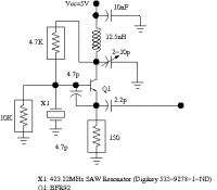
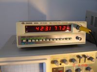
EDIT 20060615: Managed to get the low noise RF amplifier, band filter and local oscillator to work. It was particularly difficult to get the SAW resonators to...well..resonate! I tried the basic Colpitts oscillator topology, but it just would not work. The section of transmision line that leads to the first mixer would resonate at 1.3 GHz...not what I wanted! So I opted for the so-called SAW stabilised Colpitts oscillator. This uses a bog-standard LC tank in the collector circuit which resonates near 423.2MHz (the LO frequency). The SAW goes in the base circuit, where it looks like a low impedance at 433.2MHz, thereby forcing common-base operation at this frequency. It works like a charm! Rock-steady strong signal at 433.177MHz! 43kHz out, but well within the +-75kHz specified by the SAW data sheet...
The PCB looks like:

Here is the schematic:
The frequency counter was used to verify the oscillator frequency:
The oscillator frequency can be "pulled" several 10's of kHz by tuning the collector tank circuit. The circuit behaviour is a lot like the quartz-crystal oscillators so often used in HF.
The oscillator power output is about -4dBm.
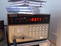
This is a bit high for the mixer input (which needs about -12 to -10 dBm). I'll use a smaller coupling capacitor (presently using 2.2pF... perhaps a 0.47pF will be enuf to give about 6dB reduction to the output signal...)
The other challenge so far is tuning up the three-element band filter (the three strips on the right). The trick is to make sure there is at least 20dB of attenuation at the "image" frequency (at 412.5MHz) and as much attenuation as possible at the LO frequency (to prevent radiation of the LO by the receiving antenna). When I get the receiver assembled, I'll make some definitive measurements of LO radiation and image rejection...
EDIT 20060623:
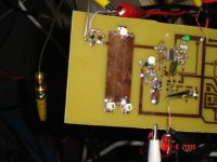
Got all the major components of the receiver to work (with the exception of the carrier regeneration subsystem). Tested the downconversion with a 384Kb/sec BPSK signal. Here is a look at the partially populated board. The Philips SA639 FM/IF chip is in the top right corner. I am capacitively coupling the oscilloscope through a high resistance (33K) through a 50 ohm cable terminated with a 50 ohm load (this reduces resonances in the coax to the o-scope input) to the output of the IF limiter. See schematic: o-scope is connected to "limiter out" pin.
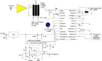
The resulting signal is at 10.7MHz with a 500KHz bandwidth (as defined by the ceramic IF filter....the white thing under the green tantalum cap in the upper right-hand corner).
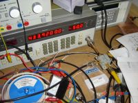
A BPSK "transmitter" is simulated using my bench RF signal generator set to 433.92MHz and a doubly balanced mixer module. The modulating signal is just a 192kHz square wave.. The RF output of the signal generator is -60dBm. The mixer suffers 10 to 14dB conversion loss, so the RF level to the receiver is around -74dBm.
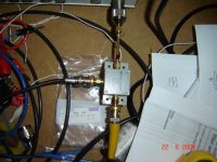
Here's a closer view of the mixer... These little modules are great....they can be a bit pricey, if you buy them new....
Here you can see the modulating "data" signal on the top trace and the output of the receiver limiter on the bottom trace. you can just make out the transtions in the IF signal.
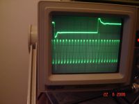
Here is an expanded version showing the phase of the 10.7MHz IF signal slewing during the bit transitions.
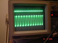
The waveform is a bit foggy because the data signal and the carrier are not synchronised to a common reference timebase. However, it is clear that the receiver circuit has properly downconverted the RF signal. I can visualise that "fuzziness" in the IF waveform down to -94dBm... The sensitivity is not too bad for the simple circuit. When I finish the demodulator, perhaps I'll see the signal at even lower levels... (I'm hoping for at least -100dBm sensitivity)...
Next step is to assemble the PLL carrier recovery circuit to complete the demodulation of the signal.
EDIT 20060628:
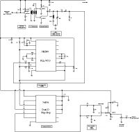
Got the PLL carrier recovery circuit to work. Here's a schematic. (This is the basic circuit.. I've replaced the bulky TO92 2N2222's with SOT (surface mount) BC848 NPN transistors... works fine! This means that the receiver is ready for experiments!
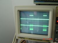
After adjusting the level and the phase of the regenerated 10.7MHz (IF) carrier, we see the data signal (192kbit/sec).
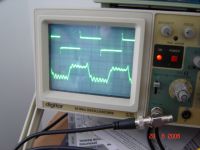
The ringing is the result of the coax I am using to conect to the o-scope. The receiver is producing a clean 96kHz "square" output with the "transmitter" power set to 10uW with random wire antennas on both receiver and transmitter spaced a couple of meters apart. The top trace is the signal generator (transmitted) "data" and the lower trace is the received "data."
What happens if we simulate a long string of "0s" or "1s"... Setting the signal generator to burst mode allows us to test this.
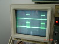
Again, upper trace is the transmitted "data" burst and the lower is the received "data". We simulate a long string of zeros here, as seen by the flat-line part of the signal. PLL lock seems to be well maintained during bit transition times, the output data signal is rock solid.
By cycling the transmitter RF on and off a few times, we can observe the 180 degree ambiguity in the regenerated carrier (which is characteristic of Costas loop and squaring loop carrier regeneration systems, like this one). Notice that the string of "zeros" now produces a "high" output signal during the flat-line stage, i.e. the received data signal is inverted..
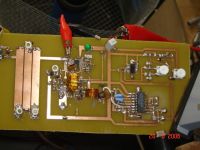
This is a shot of the completed receiver board.
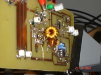
This shot shows the key component of the frequency doubler: the 1:1:1 toroidal transformer that feeds the push-push frequency doubler.
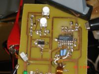
This photo shows the completed PLL-based carrier regeneration subsystem. The PLL is on the right and a 74H74 D flip-flop (frequency divide-by-2) is the chip seen on the left. The two white trimmer pots are for adjusting the phase and amplitude of the regenerated 10.7MHz carrier to be fed to the secong receiver mixer (for synchronously recovering the BPSK signal).
Lastly, we have the receiver "random wire" antenna....a white alligator clip lead. (Next step will be to put together a couple of nice 50-ohm matched antennas for 433.92MHz...this should improve low-level signal performance significantly..)
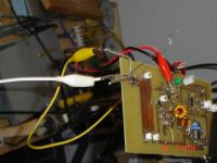
EDIT 20060629
Made an antenna... Will make another one tomorrow!
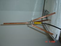
The elements ar 15.6 cm long.. Simulations indicate nearly a 50 ohm fully resistive feedpoint impedance...
EDIT 20060703
Tried to do some sensitivity tests, but it is very difficult here in the center of a major urban environment. The interference level is very high. In fact, the power meter connected to the 433 MHz (filtered) output from the LNA with the antenna attached indicates -45 to -40 dBm.. this is very high, buit expected given the noisy environment of garage door openers, electronic car keys as well as possible amateur 70cm service... However, with a Tx power of around 500uW (-3 dBm) the carrier regeneration PLL holds its lock (with occasional fading) and a 192kbit/sec signal can be recovered just about everywhere in my flat. The "tripod" antennas work like a charm...10-20dB better response than my "random wire" experiment early on...
EDIT 20060706
Modified the carrier recovery PLL loop filter. Can now stably demodulate 384kbit/sec BPSK data stream (using the full bandwidth of the ceramic IF filter). I'm happy!! Need to add a simple circuit to modify demodulated data stream to TTL levels to feed to a 5V RS-232 serial port input of a microcontroller for processing (parity check, error correction, etc.)... Still need to build the transmitter!!!
EDIT 20060710
Improvements to receiver: matching at RF input to SA639 will improve sensitivity. Would like to study effect of noise in received signal on carrier recovery PLL...
EDIT 20060830
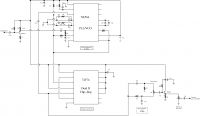
Simplified carrier recovery circuit. Frequency doubler is not needed. Use output from flip-flop and do phase comparison on 10.7MHz IF signal like this.
EDIT 20060921
Transmitted message across my flat! Very happy..
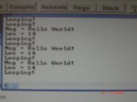
I used two Rabbit2000 processor boards. One to generate the "Hello World" message at 96kb/sec and another to receive. I used Biphase-mark Manchester encoding to synchronously transmit data (the bit clock is easily regenerated at the receive end at the cost of halving the bit rate wrt NRZ RS232 type asynchronous links). The radio link is capable of 192kbit/set using Manchester encoding, but my Rabbit processors are not fast enough and drop bits when the baud rate exceeds 115kbit/sec. Using assembly code and interrupt routines are a must (especially for the receiver).
Next step... build 3 proper transceiver boards with faster processors and start working on simple network.
Re: Low power 433 MHz BPSK data transmission system
ragnar, Tue May 30 2006, 06:38AM
Your high frequency work is always amazing, Waverider! =)
I hope you don't get into trouble with the european union / fcc
ragnar, Tue May 30 2006, 06:38AM
Your high frequency work is always amazing, Waverider! =)
I hope you don't get into trouble with the european union / fcc

Re: Low power 433 MHz BPSK data transmission system
WaveRider, Tue May 30 2006, 09:44AM
Thanks BP!
The FCC part 15 rules are far more restrictive than the EU, because 433MHz is not an ISM band in the USA.
[i]
Plugging in the numbers, you get about 43uW transmitter power (assuming an isotropic radiator) in the 260-470MHz range.
In the EU, we have
Hence, one can use 10dBm (10mW) with wide band signals if one observes a 10% transmit duty cycle. If 0dBm (1mW) is used, duty cycle is not limited...
(See this link: ).
).
Of course, if you have a suitable amateur operator's license, power limits are much higher!
Cheers!
WaveRider, Tue May 30 2006, 09:44AM
Thanks BP!
The FCC part 15 rules are far more restrictive than the EU, because 433MHz is not an ISM band in the USA.
[i]
wrote ...
Excerpted from FCC part 15, paragraph 15.231-b3e
(e) Intentional radiators may operate at a periodic rate exceeding that specified in paragraph (a) and may be employed for any type of operation, including operation prohibited in paragraph (a), provided the intentional radiator complies with the provisions of paragraphs (b) through (d) of this Section, except the field strength table in paragraph (b) is replaced by the following: __________________________________________________ ______________
- Fundamental Field Strength of Field Strength of Frequency Fundamental Spurious Emission (MHz) (microvolts/meter) (microvolts/meter)
- 40.66 - 40.70 1,000 100
- 70 - 130 500 50
- 130 - 174 500 to 1,500 50 to 150
- 174 - 260 1,500 150
- 260 - 470 1,500 to 5,000 150 to 500
- Above 470 5,000 500
Plugging in the numbers, you get about 43uW transmitter power (assuming an isotropic radiator) in the 260-470MHz range.
In the EU, we have
wrote ...
The ECC recommendation 70-03 defines both the maximum transmit power and limits to the duty cycle and the bandwidth of the transmitter for each allocated frequency band. Table 9 lists the frequencies and the limits for non-specific short range devices for the frequency range between 433 MHz and 2.4835 GHz. Table 9. Frequency Bands For Non-Specific Short Range Devices in Europe
The ECC recommendation 70-03 defines both the maximum transmit power and limits to the duty cycle and the bandwidth of the transmitter for each allocated frequency band. Table 9 lists the frequencies and the limits for non-specific short range devices for the frequency range between 433 MHz and 2.4835 GHz. Table 9. Frequency Bands For Non-Specific Short Range Devices in Europe
- Frequency band ERP Duty Cycle Channel Bandwidth Remarks
- 433.05 434.79 MHz +10 dBm <10% No limits No audio and voice
- 433.05 434.79 MHz 0 dBm No limits No limits £ 13 dBm/10 kHz, no audio and voice
- 433.05 434.79 MHz +10 dBm No limits <25 kHz No audio and voice
- 868 868.6 MHz +14 dBm < 1% No limits
- 868.7 869.2 MHz +14 dBm < 0.1% No limits
- 869.3 869.4 MHz +10 dBm No limits < 25 kHz Appropriate access protocol required
- 869.4 869.65 MHz +27 dBm < 10% < 25 kHz Channels may be combined to one high speed channel
- 869.7 -870 MHz +7 dBm No limits No limits
- 2400 2483.5 MHz +7.85 dBm No limits No limits Transmit power limit is 10-dBm EIRP
Hence, one can use 10dBm (10mW) with wide band signals if one observes a 10% transmit duty cycle. If 0dBm (1mW) is used, duty cycle is not limited...
(See this link:
 ).
).Of course, if you have a suitable amateur operator's license, power limits are much higher!
Cheers!
Re: Low power 433 MHz BPSK data transmission system
WaveRider, Thu Jun 15 2006, 02:04PM
The 423.22MHz local oscillator was a bit of a bear to get working, but I finally did it! See the updated first post if you're interested!
Those tiny SAW device packages require a steady hand to solder...
Cheers!
WaveRider, Thu Jun 15 2006, 02:04PM
The 423.22MHz local oscillator was a bit of a bear to get working, but I finally did it! See the updated first post if you're interested!
Those tiny SAW device packages require a steady hand to solder...
Cheers!
Re: Low power 433 MHz BPSK data transmission system
WaveRider, Fri Jun 23 2006, 09:16AM
omg.... the downconversion works!!
Now I need to finish the carrier recovery circuit...
WaveRider, Fri Jun 23 2006, 09:16AM
omg.... the downconversion works!!
Now I need to finish the carrier recovery circuit...
Re: Low power 433 MHz BPSK data transmission system
ragnar, Fri Jun 23 2006, 01:25PM
I look forward to it, Waverider!
I also envy your oscilloscope, hehe =)
ragnar, Fri Jun 23 2006, 01:25PM
I look forward to it, Waverider!
I also envy your oscilloscope, hehe =)
Re: Low power 433 MHz BPSK data transmission system
WaveRider, Wed Jun 28 2006, 12:11PM
Woot! Got the receiver to work!! Updated first post..
Hi BP... I like my scope too... It's only good to 20MHz, tho'... Wish I had at least a 100MHz scope...
WaveRider, Wed Jun 28 2006, 12:11PM
Woot! Got the receiver to work!! Updated first post..
Hi BP... I like my scope too... It's only good to 20MHz, tho'... Wish I had at least a 100MHz scope...
Re: Low power 433 MHz BPSK data transmission system
WaveRider, Thu Sept 21 2006, 09:37AM
Updated thread.. Got basic link protoypye to work!!
The microcontroller assembly code was a bit tricky, but got it to work...finally!
WaveRider, Thu Sept 21 2006, 09:37AM
Updated thread.. Got basic link protoypye to work!!
The microcontroller assembly code was a bit tricky, but got it to work...finally!
Re: Low power 433 MHz BPSK data transmission system
ragnar, Thu Sept 21 2006, 10:32AM
Very impressive.. do I guess you're practically finished now?
What application's this going to be for when you get the transmitter/receiver all into a box? =P
ragnar, Thu Sept 21 2006, 10:32AM
Very impressive.. do I guess you're practically finished now?
What application's this going to be for when you get the transmitter/receiver all into a box? =P
Re: Low power 433 MHz BPSK data transmission system
WaveRider, Thu Sept 21 2006, 11:08AM
Hi BP!
I want to transmit images, GPS, telemetry data from a remote location. In the next iteration of this project, I would like to up the bit rate to at least 1.2Mbit/s.. The long-term plan is to put the whole picture-taking/telemetry assembly into a high-altitude balloon much like this fellow does.
I must admit, I could go out and buy a radio module...but where is the fun in that?!

Re: Low power 433 MHz BPSK data transmission system
Chris Russell, Fri May 29 2009, 07:52PM
I'm resurrecting this thread because it is now a featured project. Excellent work, WaveRider! I had nearly forgotten about the awesome work you've done here.
Chris Russell, Fri May 29 2009, 07:52PM
I'm resurrecting this thread because it is now a featured project. Excellent work, WaveRider! I had nearly forgotten about the awesome work you've done here.
Re: Low power 433 MHz BPSK data transmission system
Proud Mary, Fri May 29 2009, 09:09PM
Very interesting indeed!
Proud Mary, Fri May 29 2009, 09:09PM
Very interesting indeed!

Re: Low power 433 MHz BPSK data transmission system
Hazmatt_(The Underdog), Fri May 29 2009, 09:43PM
totally awsome! Now to inject something silly: What's your Bit Error Rate? hehehe
Hazmatt_(The Underdog), Fri May 29 2009, 09:43PM
totally awsome! Now to inject something silly: What's your Bit Error Rate? hehehe
Re: Low power 433 MHz BPSK data transmission system
GeordieBoy, Fri May 29 2009, 10:56PM
This is an interesting project and a very good clear write-up of it on here too.
How do you plan to deal with the 180 degree phase ambiguity thing inherent with BPSK? Will you convert it to differential phase shift keying, or add some kind of preamble to the data packets to clarify the ones and zeros in the demodulated data?
Do you have access to a spectrum analyser? It would be interesting to see examples of the PSK carrier spectrum either at the 433MHz or the IF frequency.
-Richie,
Re: Low power 433 MHz BPSK data transmission system
rp181, Sat May 30 2009, 12:47AM
I have never seen this project before, very well done. Do you have any more uses for it?
Great write-up.
rp181, Sat May 30 2009, 12:47AM
I have never seen this project before, very well done. Do you have any more uses for it?
Great write-up.
Re: Low power 433 MHz BPSK data transmission system
syntroniks, Sat May 30 2009, 08:38PM
Answered my own question. Great project BTW!
syntroniks, Sat May 30 2009, 08:38PM
Answered my own question. Great project BTW!
Re: Low power 433 MHz BPSK data transmission system
timothius, Sun May 31 2009, 02:58AM
Incredible! Everything is done so elegantly - makes my circuits look so "hacky".
How do you ensure that you data is sufficiently balanced such that you don't get comparator errors? (Causing DC offsets at the comparator input)
timothius, Sun May 31 2009, 02:58AM
Incredible! Everything is done so elegantly - makes my circuits look so "hacky".
How do you ensure that you data is sufficiently balanced such that you don't get comparator errors? (Causing DC offsets at the comparator input)
Re: Low power 433 MHz BPSK data transmission system
graphic_crap, Sun Aug 09 2009, 02:47PM
hello sir
im Naman Maheshwari a final year student and willing to undertake dis very project of urs as my final year project so please can u send me d complete project description on my email id **link** i'll be really grateful to u
graphic_crap, Sun Aug 09 2009, 02:47PM
hello sir
im Naman Maheshwari a final year student and willing to undertake dis very project of urs as my final year project so please can u send me d complete project description on my email id **link** i'll be really grateful to u
Re: Low power 433 MHz BPSK data transmission system
aonomus, Sun Aug 09 2009, 04:43PM
Out of curiosity, is the reverse of your board a solid ground plane? How did you do impedence controlled routing without grounds on either side of the major signal paths (or does it not matter at your power level?).
aonomus, Sun Aug 09 2009, 04:43PM
Out of curiosity, is the reverse of your board a solid ground plane? How did you do impedence controlled routing without grounds on either side of the major signal paths (or does it not matter at your power level?).
Re: Low power 433 MHz BPSK data transmission system
WaveRider, Wed Aug 12 2009, 03:08PM
Thanks for the comments!
Aonomus: Yes, the back of the board is a solid ground plane, so all lines can be impedance controlled and radiation from the board is minimised.
Also, the phase ambiguity can be easily handled by using differential BPSK.
Note: the sensitivity of the receiver is not quite what I had hoped because the SA639 has a limiter built in which in low SNR (or high interference) situations, "loses" the desired signal and is swamped with noise. I was lucky to get -80dBm sensitivity in the end. The "right" way to do this would be to lose the limiter stage and use a proper AGC so the PLL carrier recovery would have some component of the weak desired signal to lock on to. I may get around to this in a later project....maybe at 2.4GHz.. ALl-in-all I found it an instructive project.
Cheers!
Re: Low power 433 MHz BPSK data transmission system
vaio007, Wed Mar 31 2010, 03:12PM
What type of transmitter you will be use?
vaio007, Wed Mar 31 2010, 03:12PM
What type of transmitter you will be use?
Print this page